Method and apparatus for facilitating variation-aware parasitic extraction

a technology of variation awareness and extraction method, applied in the direction of cad techniques, stochastic cad, instruments, etc., can solve the problems of large number of interconnection template requirements, large computation requirements for generating capacitance tables, and enormous time-consuming process

Active Publication Date: 2009-09-08
SYNOPSYS INC
View PDF6 Cites 9 Cited by
  • Summary
  • Abstract
  • Description
  • Claims
  • Application Information

AI Technical Summary

Benefits of technology

[0011]One embodiment of the present invention provides an approach to efficiently and accurately generate statistical sensitivity coefficients to complement the nominal capacitance tables and to use the statistical sensitivity coefficients for variation-aware parasitic extraction.
[0012]An embodiment of the present invention does not generate capacitance tables for different process corners. Instead, the embodiment efficiently generates statistical sensitivity coefficients which model the expected change in an electrical property (e.g., capacitance) due to variations in an interconnect process parameter value (e.g., dielectric thickness). Note that, a sensitivity coefficient with respect to a process parameter is the fractional change of an electrical property value due to a unit variation in the process parameter.
[0013]The nominal electrical property tables along with the associated statistical sensitivity coefficients can provide the necessary and sufficient coverage for all possible effects of parameter variations on an electrical property. In this way, embodiments of the present invention can provide a practical technique to cover all possible ranges of random parameter variation.
[0015]In one embodiment, the system first generates the set of nominal capacitance tables. This usually involves a numerical discretization process to set up the simultaneous algebraic equations, a matrix factorization process, and substitution steps to obtain the nominal capacitance tables. Next, the system determines statistical sensitivity coefficients by reusing significant portions of the intermediate results that were generated during the nominal capacitance computations. This aspect of the present invention enables the system to generate sensitivity coefficients by using a substantially small amount of computation.

Problems solved by technology

Unfortunately, generating capacitance tables typically requires vast amounts of computation because of at least two reasons.
First, a large number of interconnect templates are required to adequately cover the geometries that are usually encountered in an integrated circuit.
Second, determining the parasitic capacitance for each interconnect template involves generating and solving large sets of simultaneous linear equations.
This can be an enormously time consuming process even for today's high performance computers.
Furthermore, advances in process technologies are expected to result in more complex geometries, larger number of metal layers, and more stringent accuracy requirements.
All of these developments will further increase the computational demands.
Unfortunately, process parameters often vary from their nominal values due to random variations in the manufacturing processes.
It is evident that such approaches will require an almost infeasible amount of computation.
Hence, for all practical purposes, generating capacitance tables for a sufficiently large number of process corners is computationally infeasible.
To overcome the computational burden, some prior art techniques sacrifice accuracy.
Unfortunately, the perfect correlation assumption is unrealistic because these process steps occur at different times in the fabrication flow, and hence are independent of one another.
Further, there is no guarantee that the combinations of extreme parameter variations cover the actual best-case or worst-case scenarios in terms of timing delay or crosstalk analysis.

Method used


Image

  • Method and apparatus for facilitating variation-aware parasitic extraction
  • Method and apparatus for facilitating variation-aware parasitic extraction
  • Method and apparatus for facilitating variation-aware parasitic extraction

Examples


Embodiment Construction

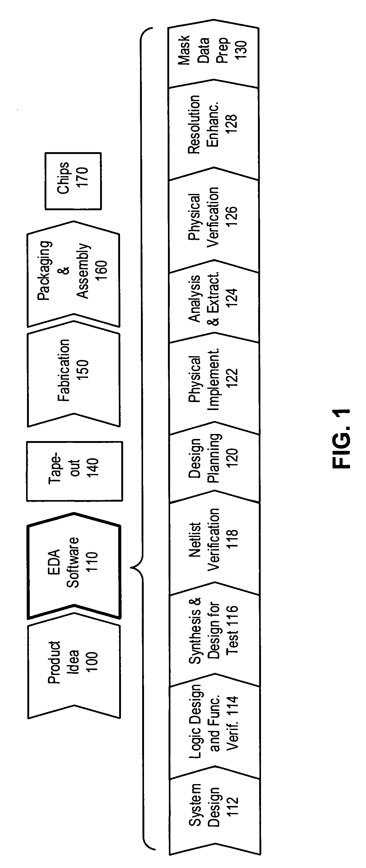
Integrated Circuit Design Flow

[0024]FIG. 1 illustrates various steps in the design and fabrication of an integrated circuit in accordance with an embodiment of the present invention.

[0025]The process can start with the conception of the product idea (step 100) which may be realized using an EDA design process (step 110). When the design is finalized, it can be taped-out (event 140). After tape out, the fabrication process (step 150) and packaging and assembly processes (step 160) are performed which ultimately result in finished chips (result 170).

[0026]The EDA design process (step 110), in turn, can comprise steps 112-130, which are described below. Note that the design flow description is for illustration purposes only. This description is not meant to limit the present invention. For example, an actual integrated circuit design may require the designer to perform the design steps in a different sequence than the sequence described below. The following discussion provides further ...


PUM


Abstract

One embodiment of the present invention provides a system for determining an electrical property for an interconnect layer. During operation, the system receives interconnect technology data which includes nominal parameter values for a first interconnect layer, and parameter-variation values which represent variations in the nominal parameter values due to random process variations. Next, the system receives an interconnect template which describes the geometry of a portion of a second interconnect layer. The system then determines electrical property data for the interconnect template using the interconnect technology data. The electrical property data can include a nominal electrical property value, and sensitivity values which represent the sensitivities of the nominal electrical property value to variations in the nominal parameter values. Next, the system stores the electrical property data and the interconnect technology data in a storage.

Description

RELATED APPLICATION[0001]This application hereby claims priority under 35 U.S.C. §119 to U.S. Provisional Patent Application No. 60 / 740,487, filed on 29 Nov. 2005, entitled “Efficient generation and representation of statistical sensitivity coefficients for variation-aware parasitic extraction,” by inventors Edhi Sutjahjo, Kishore Singhal, Byungwook Kim, Baribrata Biswas, Alex Gyure, and Mahmoud Shahram, the contents of which are herein incorporated by reference.BACKGROUND[0002]1. Field of the Invention[0003]The present invention relates to semiconductor design and manufacturing. More specifically, the present invention relates to a method and an apparatus for facilitating variation-aware parasitic extraction.[0004]2. Related Art[0005]Process variation related yield loss is becoming dominant in nanometer technologies. Higher circuit speeds and increasing relative variations in the design parameters have created a strong need for variation-aware tools, such as, variation aware static...

Claims


Application Information

Patent Timeline
Patent Type & Authority Patents(United States)
IPC IPC(8): G06F17/50
CPCG06F17/5018G06F17/5036G06F2217/78G06F2217/10G06F30/23G06F30/367G06F2111/08G06F2119/06
Inventor SUTJAHJO, EDHISINGHAL, KISHOREKIM, BYUNGWOOKLEONHARDT, GOETZQIU, BEIFANGKRASNOVSKY, SERGEYBISWAS, BARIBRATAGYURE, ALEXSHAHRAM, MAHMOUD
Owner SYNOPSYS INC
Why Eureka
Try Eureka