Many devices, particularly MEMS do not function properly when embedded in a completely
solid environment.
Freedom to move during operation would be lost if these elements were simply left embedded in a
solid film deposited over the substrate as is commonly done in the
microelectronics industry.
The type of
package employed for such a MEMS or microelectronic device greatly affects their cost and functionality.
This type of packaging is not
wafer-level and is limited to stand-alone (discrete) devices, and therefore is expensive.
Fabrication of microcap packages of the type shown is frequently more expensive than the fabrication of the devices they protect.
Fabrication and alignment of second substrate 105 is costly and, as shown, seal ring 110 requires a significant amount of die area, thereby increasing the cost by limiting the minimum dimension of the
package.
Thus, the microcap
package limits the scaling of the packaged device, accounts for a large percentage of the packaged device cost and limits
wafer-level integration of devices requiring a fluidic environment with those that do not.
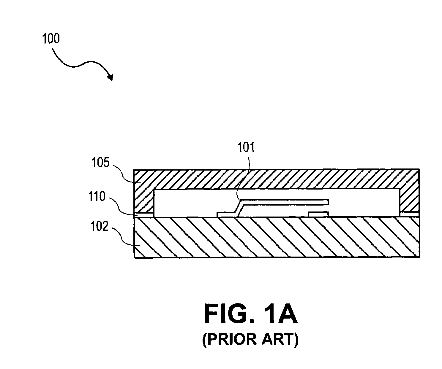
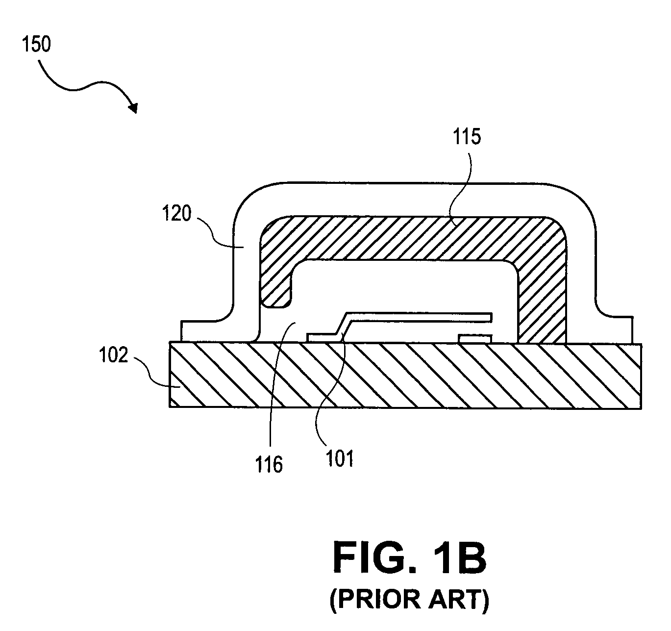
However, one issue with the conventional microshells is that the pressure inside the microshell is not controllable as in the microcap
bonding process.
Sealing the microshell with a
silicon dioxide process typically limits the level of vacuum that can be achieved within the microshell and can result in
contamination on the encapsulated device.
Furthermore, conventional microshells are not as robust as bonded microcap packages and so, as the chamber size is increased, are not readily capable of withstanding the pressure of the final package molding process employed in conventional
microelectronics, which is on the order of 1000
pounds per square inch (PSI).
Therefore, the cost of the final package encompassing the conventional microshell can remain high.
For this reason too, it is not easy to monolithically integrate a conventional microshell with microelectronic devices (eg.
Still another limitation of conventional microshells is that non-conventional processes are typically employed which either increase costs or render the package incompatible with microelectronics.
This
etching of high
aspect ratio perforations 116 through a non-porous pre-sealing layer can be very difficult because non-planarity, as shown in FIG. 1B, limits the minimum resolvable aperture
diameter for a given
exposure wavelength.
Moreover, process difficulties associated with
etching high
aspect ratio apertures (such as etch stop, etc.) increase the cost of forming the high
aspect ratio perforation 116 in conventional thin film encapsulated package 150.
Furthermore, many conventional microshells require high temperature
processing that is incompatible with microelectronic devices.
Because modern
CMOS transistors typically have a low thermal budget, any
processing of a significant duration at much over 650° C. will degrade
transistor performance.
Thus, integration of a microshell with
CMOS can not easily be accomplished.
Thus, monolithically integrating the conventional microshell with microelectronics is again severely limited.

