Electromagnetic wave generation apparatus and manufacturing method of electromagnetic wave generation apparatus

a technology of electromagnetic wave generation and electromagnetic wave, which is applied in the direction of sustainable manufacturing/processing, final product manufacturing, electric discharge tube/lamp manufacturing, etc., can solve the problems of generating leakage current, unable to meet the requirements of environmental temperature or certain applications, and the size of such apparatus becomes inevitably big

Inactive Publication Date: 2009-09-29
PANASONIC CORP
View PDF6 Cites 3 Cited by
  • Summary
  • Abstract
  • Description
  • Claims
  • Application Information

AI Technical Summary

Benefits of technology

[0010]The present invention is conceived considering the above-described problems. An object of the present invention is to provide a compact electromagnetic wave generation apparatus that generates a high power terahertz wave and a manufacturing method of the electromagnetic wave generation apparatus.
[0036]The present invention can provide an electromagnetic generation apparatus that is compact and generates a high power terahertz wave and manufacturing methods of the electromagnetic generation apparatus.FURTHER INFORMATION ABOUT TECHNICAL BACKGROUND TO THIS APPLICATION

Problems solved by technology

However, the method described in the Reference Document 2 is not effective at certain environmental temperatures or in certain applications.
In addition, the method requires a terahertz wave generation apparatus having a cooler, and thus the size of such apparatus becomes inevitably big because of the cooler.
Also, even in using the apparatus for a short time, increase in voltage to be applied to between both the electrodes resulting in generation of leakage current that is conducted by hopping the surface level of the GaAs layer 92.
This leakage current is a cause of decrease in the generation efficiency of a terahertz wave.

Method used


Image

  • Electromagnetic wave generation apparatus and manufacturing method of electromagnetic wave generation apparatus
  • Electromagnetic wave generation apparatus and manufacturing method of electromagnetic wave generation apparatus
  • Electromagnetic wave generation apparatus and manufacturing method of electromagnetic wave generation apparatus

Examples


first embodiment

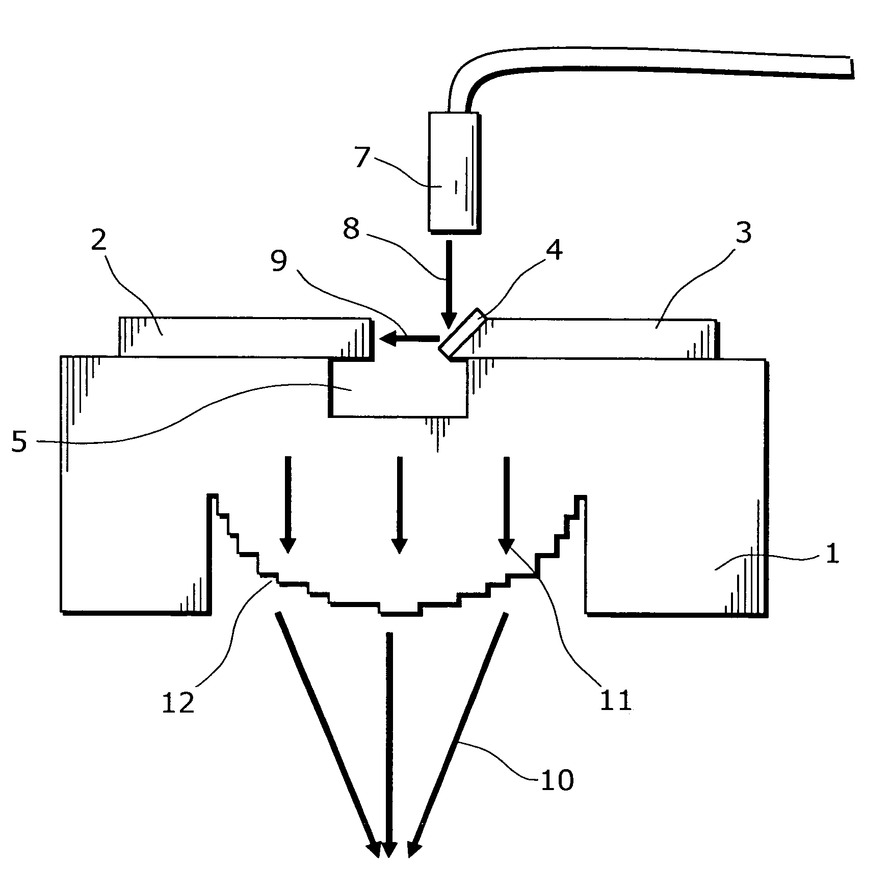
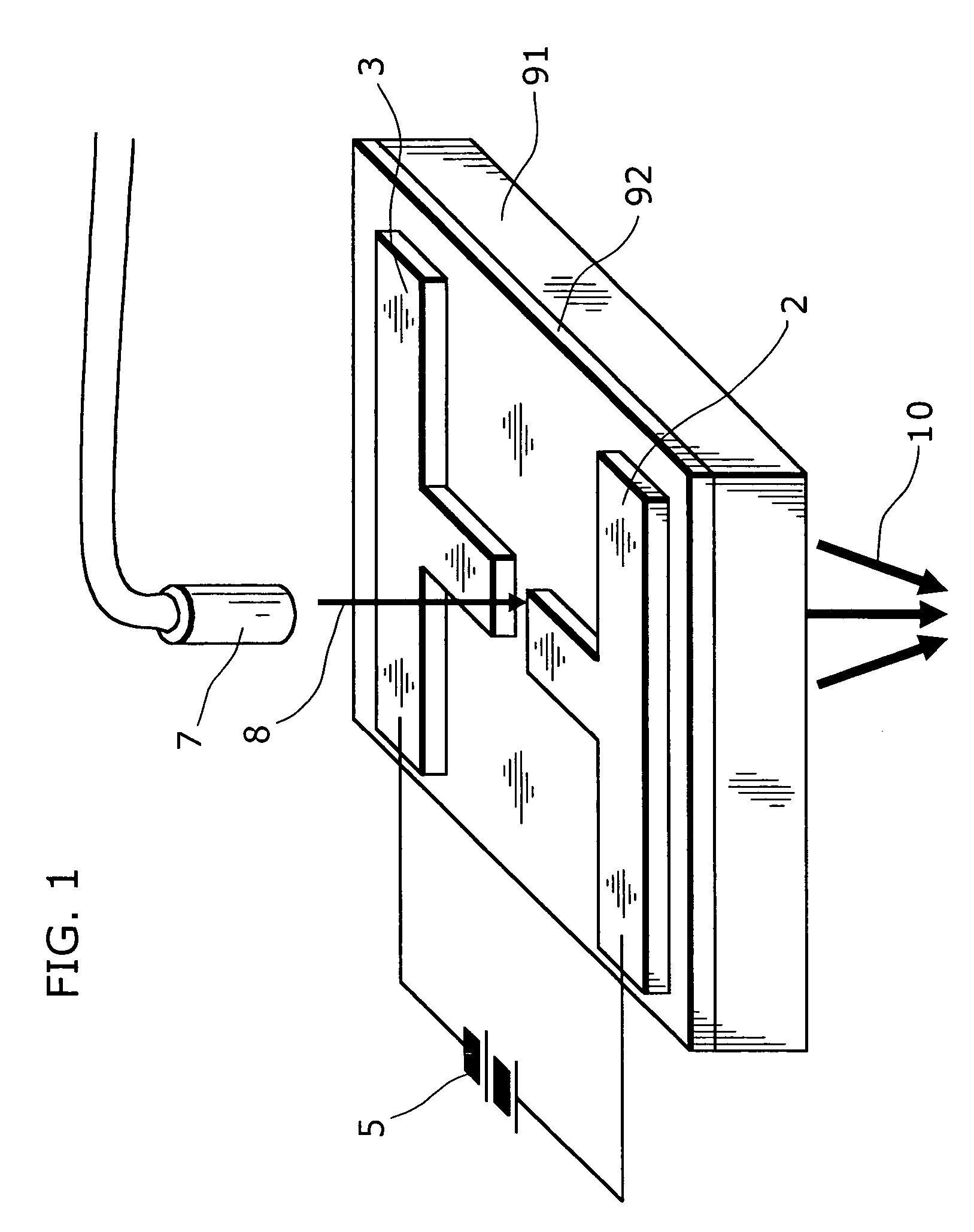
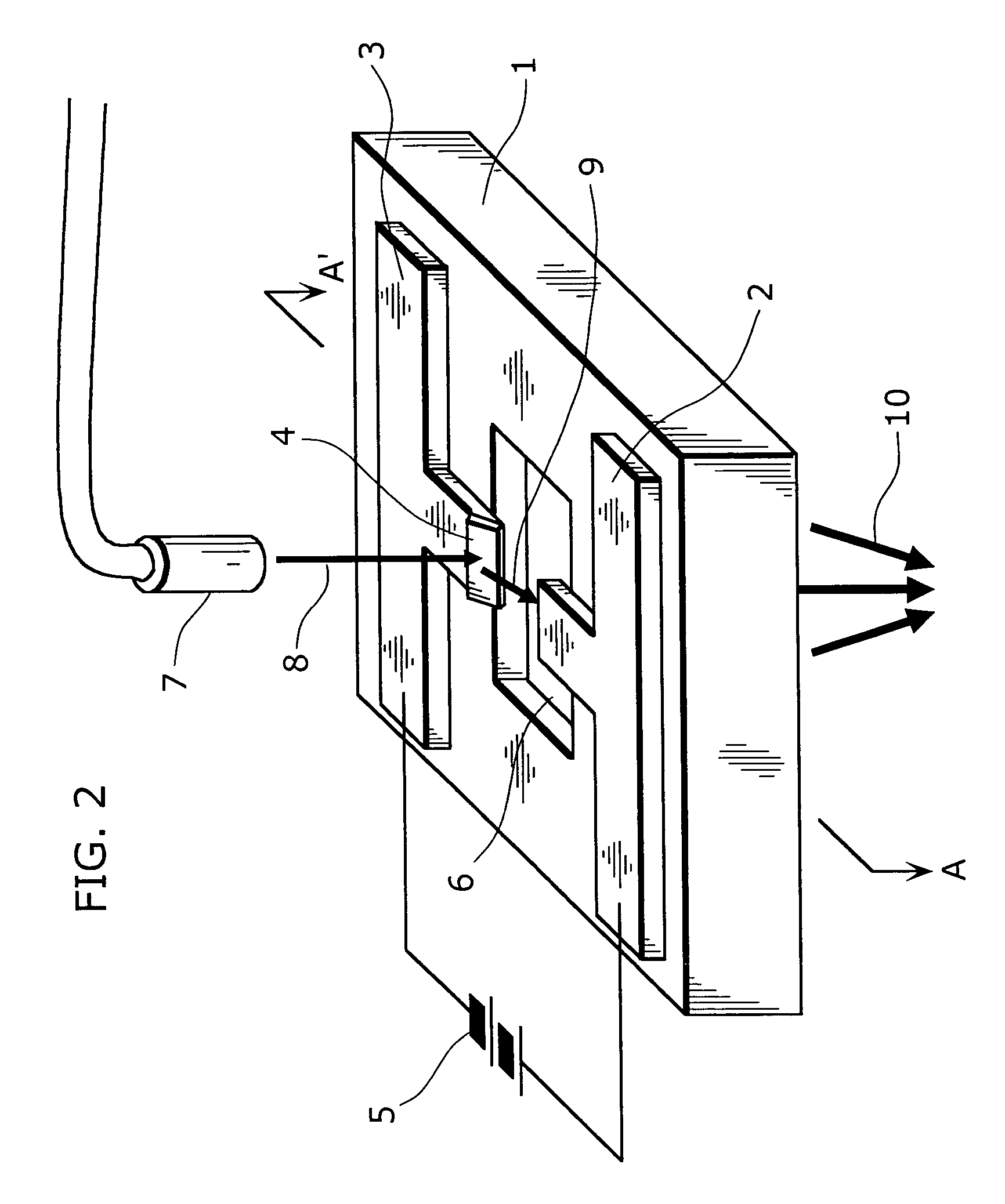
[0058]First, a terahertz wave resonator of a first embodiment will be described with reference to FIG. 2 to FIGS. 7A to 7E. The terahertz wave resonator is an example of an electromagnetic wave generation apparatus of the present invention.

[0059]FIG. 2 is a perspective view of the terahertz wave resonator in the first embodiment. FIG. 3 is a section view A to A′ of the resonator.

[0060]A positive electrode 2 and a negative electrode 3 are formed on silicon substrate 1 having a high resistance. The positive electrode 2 and the negative electrode 3 each is formed using gold, has a plate shape, and has a thickness of 0.2 μm. The positive electrode 2 and the negative electrode 3 each is formed to become T-shaped by means of photolithography. The length of the vertical line in T is 150 μm and the length of the corresponding horizontal line is 2 mm. There is a gap d of 2 μm between the positive electrode 2 and the negative electrode 3. The positive electrode 2 and the negative electrode 3 ...

second embodiment

[0077]FIG. 8 is a perspective view of a terahertz wave resonator in a second embodiment. FIG. 9 shows the section view B to B′ of the terahertz wave resonator. An incident light 8 in FIG. 9 is actually present in the vertical direction shown in the paper sheet, however, for simplification, it is shown in the same surface as the section view of the resonator.

[0078]A conductive epitaxial layer 24 is formed on a part of the semi-insulating SiC substrate 27. On the conductive epitaxial layer 24 a CNT electron emitter 22 is formed, the emitter being composed of carbon nano tubes (CNT). A negative electrode 3 is formed on the conductive epitaxial layer 24 through a contact part 26. An electron catching unit 25 is formed facing the CNT electron emitter 22 through the SiO2 spacer layer 23. The electron catching unit 25 is connected to the positive electrode 2. A power supply 5 applies voltage to between the positive electron 2 and the negative electron 3. An aluminum mirror 21 is formed on ...

third embodiment

[0086]FIG. 12 is a perspective view of a terahertz wave resonator in a third embodiment. FIG. 13 each shows the section view C to C′ of the terahertz wave resonator. An incident light 8 in FIG. 13 is actually present in the vertical direction shown in the paper sheet, however, for simplification, it is shown in the same surface as the section view of the resonator.

[0087]A layer 101 (simply called AlN 101 hereinafter), which is made of aluminum nitride (AlN) into which silicon is doped, is formed on a part of a semi-insulating SiC substrate 27. It is known that AlN into which silicon is doped emits electrons under a low threshold voltage (refer to pp. 1835 to 1837 of Appl. Phys. Lett. 78 (2001), by M. Kasu and N. Kobayashi). Therefore, AlN 101 functions as an electron emitter. A negative electrode 3 is formed on the AlN 101 through a contact part 26. An electron catching part 25 is formed facing the AlN 101 through a SiO2 spacer layer 23. The electron catching part 25 is connected to...


PUM


Abstract

The present invention provides an electromagnetic wave generation apparatus that is compact and generates a high power terahertz wave. An electromagnetic wave generation apparatus includes: a substrate; a first electrode, having a photoelectron emitting part, formed on one of the surfaces of the substrate; a second electrode formed on the surface of the substrate; a power supply source that applies voltage to between the first electrode and the second electrode so that the potential of the second electrode becomes higher than the potential of the first electrode; and a light source that radiates one of time modulated light and wavelength modulated light, and in the apparatus, the photoelectron emitting part (a) emits electrons when light is irradiated and (b) is placed at a position which an incident light from the light source enters and from which the emitted electrons run to the electron incidence plane of the second electrode.

Description

BACKGROUND OF THE INVENTION[0001](1) Field of the Invention[0002]The present invention relates to a generation technique of a terahertz (THz) electromagnetic wave.[0003](2) Description of the Related Art[0004]Electromagnetic waves which have a frequency ranging from 0.1 THz to 10 THz (in the terahertz region) belong to a boundary between light and electric waves. They have the following characteristics: transmitability which is a characteristic of electric waves; and telecentricity which is a characteristic of light. Also, an electromagnetic wave in such region (called “terahertz wave” hereinafter) has a number of absorption spectrums each of which is unique to a substance. Therefore, it is expected that terahertz waves are used in a number of industrial fields such as medical applications, environmental measurements and engineering applications. They include especially: an inspection of an object in an envelop; a food inspection; an inspection of personal belongings; a drug analysi...

Claims


Application Information

Patent Timeline
Patent Type & Authority Patents(United States)
IPC IPC(8): H01L29/12
CPCH01J9/244H01J21/04H01L31/09H01L31/03048Y02E10/544Y02P70/50
Inventor TAKIGAWA, SHINICHIUEDA, DAISUKE
Owner PANASONIC CORP
Why Eureka
Try Eureka