Method for fabricating pixel structure

Active Publication Date: 2009-10-06
AU OPTRONICS CORP
View PDF9 Cites 9 Cited by
  • Summary
  • Abstract
  • Description
  • Claims
  • Application Information

AI Technical Summary

Benefits of technology

[0011]The present invention is directed to a method for fabricating

Problems solved by technology

The procedures are complicated and thus require a higher fabricating cost.
Since ma

Method used


Image

  • Method for fabricating pixel structure
  • Method for fabricating pixel structure
  • Method for fabricating pixel structure

Examples


Embodiment Construction

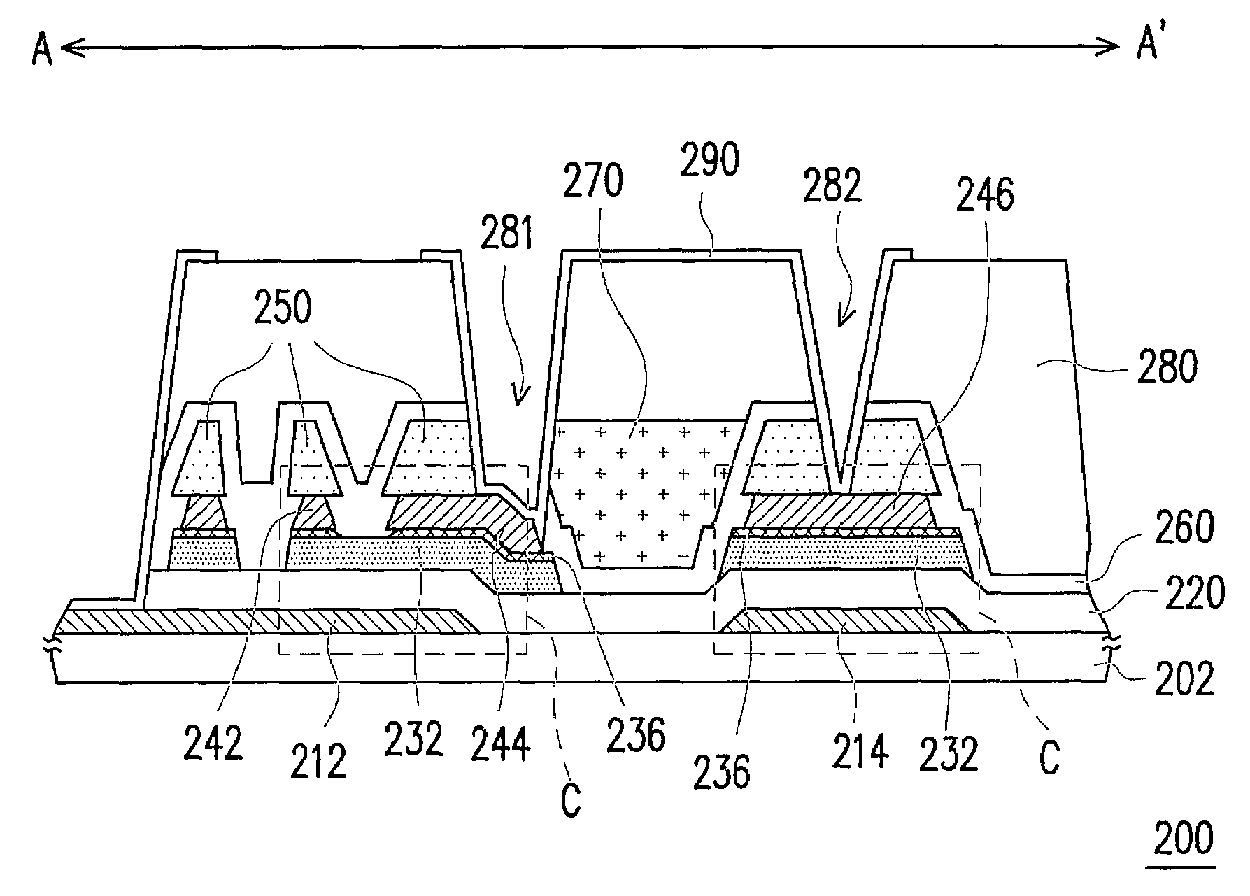
[0027]FIGS. 2A through 2H are schematic views showing a process flowchart of fabricating a pixel structure according to the present invention. FIGS. 2A′, 2E′, 2G′ and 2H′ are top views of FIGS. 2A, 2E, 2G and 2H, respectively. Specifically, FIGS. 2A′, 2E′, 2G′ and 2H′ are schematic cross-sectional views of FIGS. 2A, 2E, 2G and 2H along lines AA′ respectively. Referring to FIGS. 2A and 2A′, a substrate 202 is provided first. A material of the substrate 202 includes glass, plastic, and other rigid or soft materials, for example. Next, a gate 212 is formed on the substrate 202. The gate 212 is fabricated by forming a conductive layer (not shown) on an entire surface of the substrate 212 first through sputtering, evaporation or other thin film deposition techniques and then performing a patterning process. The aforesaid patterning process is, for example, a photolithography and etching process (PEP). Additionally, while forming the gate 212 in the present embodiment, a first capacitor e...


PUM


Abstract

A fabricating method for a pixel structure including following procedures is provided. First, a gate and a gate insulator layer are formed sequentially on a substrate. Next, a semiconductor layer, a conductive layer and a photosensitive black matrix having a color filter containing opening are sequentially formed on the gate insulator layer. The photosensitive black matrix includes a first portion and a second portion. A thickness of the first portion is smaller than that of the second portion. A channel, a source and a drain are formed simultaneously using the photosensitive black matrix as a mask. A passivation is formed on the substrate, and a color filer layer is formed within the color filter containing opening via an inkjet printing process and a dielectric layer is formed thereon. Next, a patterning process is applied to expose the drain. Ultimately, a pixel electrode connected to the drain is formed.

Description

CROSS-REFERENCE TO RELATED APPLICATION[0001]This application claims the priority benefit of Taiwan application serial no. 97120446, filed on Jun. 2, 2008. The entirety of the above-mentioned patent application is hereby incorporated by reference herein and made a part of specification.BACKGROUND OF THE INVENTION[0002]1. Field of the Invention[0003]The present invention is related to a method for fabricating a pixel structure, and particularly to a method using less photolithography and etching processes (PEP) to fabricate a pixel structure having a color filter layer.[0004]2. Description of Related Art[0005]With the advantages of high definition, small volume, light weight, low driving voltage, low power consumption and extensive application, the liquid crystal display (LCD) has replaced the cathode ray tube (CRT) as the mainstream of newly developed displays. The conventional LCD panel consists of a color filter substrate have a color filter layer, a thin film transistor (TFT) arra...

Claims


Application Information

Patent Timeline
IPC IPC(8): H01L21/00
CPCG02F1/136209H01L27/1288H01L27/1248G02F1/136227H01L29/41733G02F2001/136222G02F1/136222
Inventor YU, CHOU-HUANCHIANG, CHUN-YITSAI, CHIA-CHITUNG, CHEN-PANGHSIAO, HSIANG-CHIHCHANG, CHIA-MINGJHANG, ZONG-LONGLAI, CHE-YUNGCHOU, HAN-TANGCHANG, JUN-KAILIAO, TA-WEN
Owner AU OPTRONICS CORP
Why Eureka
Try Eureka