
Surface acoustic wave device, surface acoustic wave apparatus, and communications equipment

a surface acoustic wave and acoustic wave technology, applied in the direction of semiconductor devices, electrical equipment, electric/electrostrictive/magnetostrictive devices, etc., can solve the problems of destroying the device, affecting the service life of the device, and the isolation characteristics between the filters cannot meet the requirements of the communication terminal, etc., to achieve good out-of-band attenuation characteristics, reduce the size and height, and reduce the effect of thickness

Inactive Publication Date: 2009-10-27
KYOCERA CORP
View PDF22 Cites 26 Cited by
  • Summary
  • Abstract
  • Description
  • Claims
  • Application Information

AI Technical Summary

Benefits of technology

The present invention relates to a surface acoustic wave device that can reduce parasitic capacitance and improve out-of-band attenuation characteristics. By using a second substrate with a lower dielectric constant than the first substrate, the effective dielectric constant of the substrate can be reduced, resulting in lowered parasitic capacitance and improved isolation characteristics. Additionally, the conductor layer formed on the second substrate can efficiently discharge charges induced by rapid hysteresis in manufacturing processes. The invention also provides a branching filter with improved isolation characteristics.

Problems solved by technology

When a device having an IDT electrode on a piezoelectric substrate is passed through a step in which there is a rapid temperature change while being manufactured, sparks are generated between electrode sections in the IDT electrode, thereby destroying the device.
When the transmission-side filter and the receiving-side filter are actually formed on the same piezoelectric substrate, however, isolation characteristics between both filters cannot satisfy requirement specifications in a communications terminal.
It is considered that one cause of degradation of the isolation characteristics between the filters is leakage of an elastic wave.
Therefore, it is impossible to fulfill a miniaturization requirement.
However, this measure does not sufficiently improve the isolation characteristics.
Therefore, extra steps are required to ground a portion from the reverse surface conductor layer to the ground electrode on the main surface of the mounting substrate, thereby increasing manufacturing costs are high.

Method used


Image

  • Surface acoustic wave device, surface acoustic wave apparatus, and communications equipment
  • Surface acoustic wave device, surface acoustic wave apparatus, and communications equipment
  • Surface acoustic wave device, surface acoustic wave apparatus, and communications equipment

Examples


example

[0173]An example in which a surface acoustic wave filter that is the surface acoustic wave apparatus shown in FIG. 6 is specifically produced by way of trial using the surface acoustic wave device 1A shown in FIG. 7.

[0174]The other main surface of a piezoelectric substrate 2 and one main surface of a second substrate 21 were joined using a vitreous member composed of quartz glass as an adhesive layer 23 or a piezoelectric substrate 2 (125 μm in thickness) of a piezoelectric member composed of a 38.7-degree Y-cut X-propagation lithium tantalate (LT) single crystal. Used as the second substrate 21 was a quartz substrate having a dielectric constant εr of 4.5. The dielectric constant 4.5 was lower than the dielectric constant 42.7 of a lithium tantalate single crystal substrate.

[0175]On one main surface of the piezoelectric substrate 2, four conductor layers respectively composed of Ti, Al-1 mass percent Cu, Ti, and Al-1 mass percent Cu were deposited in this order on the side of the s...


PUM


Abstract

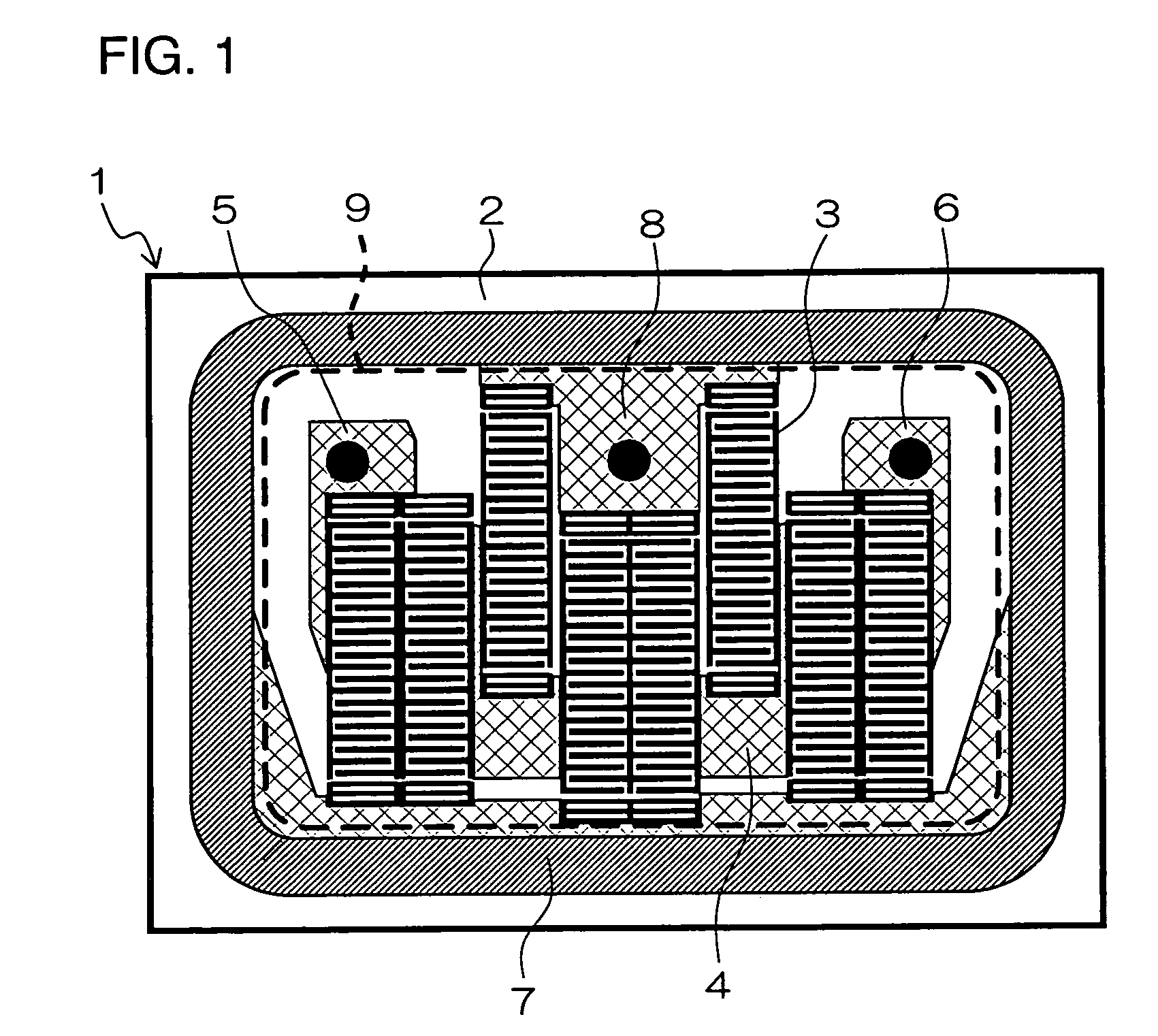
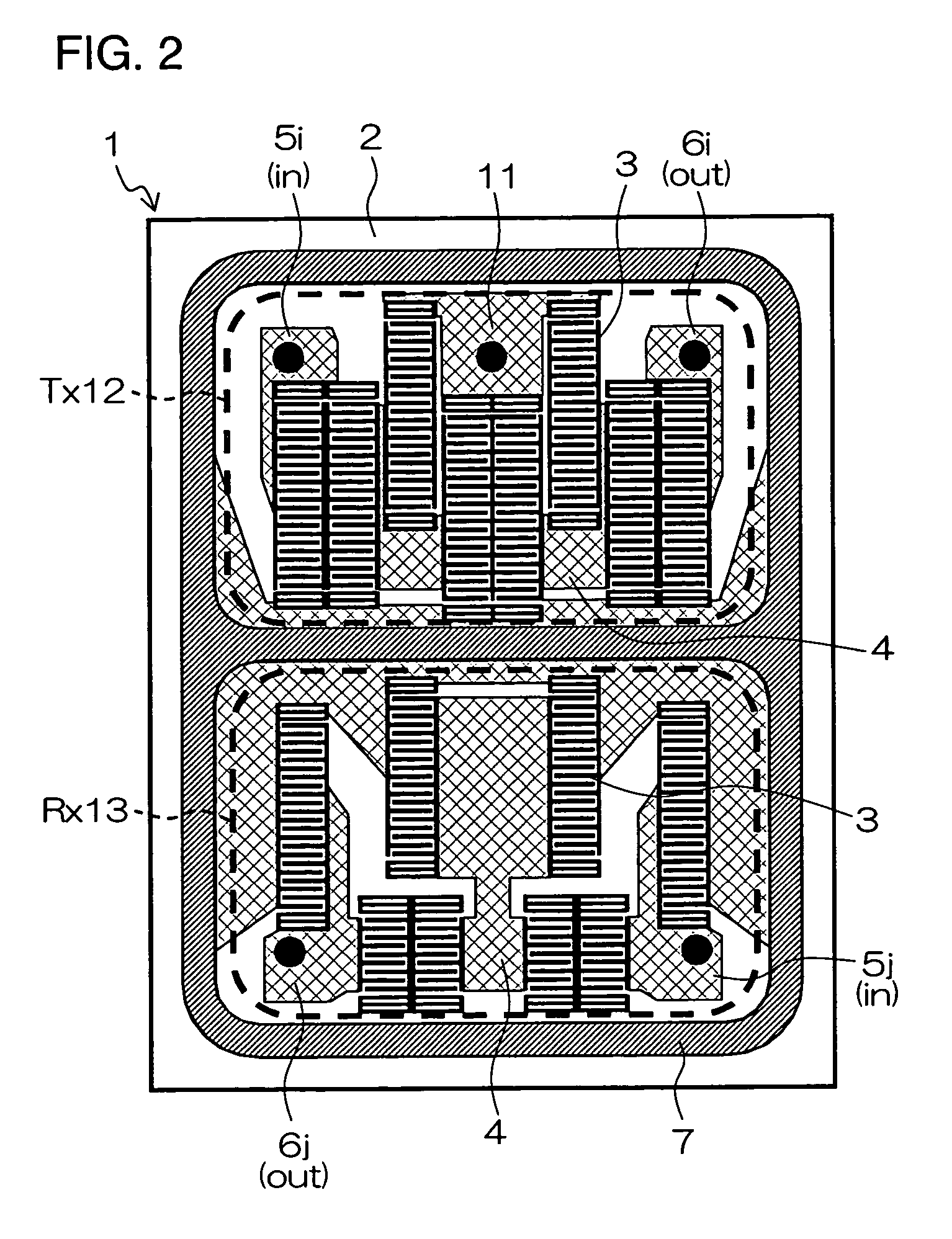
A second substrate 21 composed of a material having a lower dielectric constant than that of a piezoelectric substrate 2 having a transmission-side filter region 12 and a receiving-side filter region 13 formed therein is joined to the other main surface of the piezoelectric substrate 2, and a conductor layer 22 is formed throughout the other main surface of the second substrate 21. The effective dielectric constant of the substrate is reduced, thereby making it possible to reduce a parasitic capacitance formed between an input electrode section 5 in the transmission-side filter region 12 and an output electrode section 6 in the receiving-side filter region 13 and to improve isolation characteristics.

Description

BACKGROUND OF THE INVENTION[0001]1. Field of the Invention[0002]The present invention relates to a surface acoustic wave device employed as a high-frequency filter or the like, a surface acoustic wave apparatus, and communications equipment.[0003]2. Description of Related Art[0004]In recent years, surface acoustic wave filters have been employed for various types of communications equipment.[0005]As the frequency and the function of the communications equipment have increased, a request to increase the out-of-band attenuation of the surface acoustic wave filter has progressively increased.[0006]A schematic sectional view of a face-down mounting structure of a conventional surface acoustic wave device is illustrated in FIG. 13.[0007]In FIG. 13, reference numeral 51 denotes a piezoelectric substrate, reference numeral 52 denotes a ground pad, reference numeral 53 denotes an IDT (Inter Digital Transducer) electrode (referred to as an IDT electrode) in a comb shape formed on the piezoel...

Claims


Application Information

Patent Timeline
Patent Type & Authority Patents(United States)
IPC IPC(8): H03H9/72H03H9/05H03H9/64
CPCH03H9/02574H03H9/02614H03H9/02952H03H9/02984H03H9/725H03H9/059H03H9/1085H03H9/1092H03H9/72H03H9/0576H01L2224/16225
Inventor YOKOTA, YUUKOYAMAGATA, YOSHIFUMIIIOKA, KIYOHIRO
Owner KYOCERA CORP
Learn More