Pyramidal photonic crystal light emitting device

a photonic crystal and light-emitting device technology, applied in the direction of semiconductor devices, basic electric elements, electrical equipment, etc., can solve the problems of poor colour gamut, high voltage requirements, environmental recycling and manufacture, etc., and achieve the effect of low cost and greater uniformity and repeatability of fabrication methods

Active Publication Date: 2009-11-10
QUANTUM NIL LTD +1
View PDF10 Cites 28 Cited by
  • Summary
  • Abstract
  • Description
  • Claims
  • Application Information

AI Technical Summary

Benefits of technology

[0018]A Lambertian source emits a luminous flux per unit solid angle that in any direction is proportional to the cosine of the angle between that direction and the normal to the surface from which it is emitted. This leads to a uniform radiance with a spherical distribution. An LED comprising a structure according to the present invention combines greater directionality of emitted light with an improvement in the efficiency with which light generated by the device is coupled into the emitted beam. This is achieved through the innovative tiling arrangement of pyramidal, or frustro-pyramidal, surface projections.
[0051]Thus, the present invention also provides a simplified method of manufacture of a photonic crystal type LED structure, whereby the definition of a large feature photonic crystal is transferred onto an LED by the use of low cost photolithography or similar process and without the need for complex polishing processes.

Problems solved by technology

Currently, most LCD panels employ compact cathode fluorescent light (ccfl) sources However, these sources suffer from several problems, including poor colour gamut, environmental recycling and manufacture issues, thickness and profile, high voltage requirements, poor thermal management, weight and high power consumption In order to alleviate these problems LCD manufacturers are implementing LED BLU units.
However, for larger LCD panels, for example greater than 32 inches, the number of LEDs required to distribute the light evenly across the back of the LCD panel no longer makes this approach cost effective In U.S. Pat. No. 7,052,152 it is proposed that 124 LEDs are employed for a 32 inch LCD panel display.
Conventional High Intensity Discharge (HID) type projector light engines have always been hindered by low efficiency and short lifetime, resulting in slow adoption into consumer markets.
One of the main limiting factors reducing the efficiency of light extraction from an LED is total internal reflection of the emitted photons and their trapping in the high refractive index of the epi-material forming the LED.
However, the total light extraction for many of these photonic crystal LEDs is not as high as for more conventional surface-roughened LEDs.
In both cases the processing involves many complex and expensive steps that ultimately affect the yield and cost of the LED wafers.
One of the complex processing steps involved is the polishing of the wafers, which can adversely affect the yield due to the difficulty in controlling the surface quality across the complete wafer.
Small scratches across the surface may affect the current spreading across the LED wafer and ultimately provide a path to short circuiting the complete LED or adversely affecting the forward voltage.
By using a polishing process, poor control over the absolute thickness of the LED structure is achieved, which ultimately affects the overall output of the LED wafers from one processing batch to another.
The former technique is currently not a proven technique for such small-scale features on LED wafers and only low yields are achieved.
In addition, the technique suffers from a higher cost for small manufacturing volumes.
The latter lithography technique suffers from complex alignment and stability as well as low volumes.

Method used


Image

  • Pyramidal photonic crystal light emitting device
  • Pyramidal photonic crystal light emitting device
  • Pyramidal photonic crystal light emitting device

Examples


Embodiment Construction

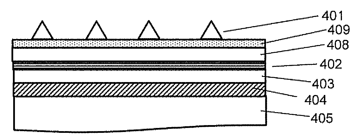
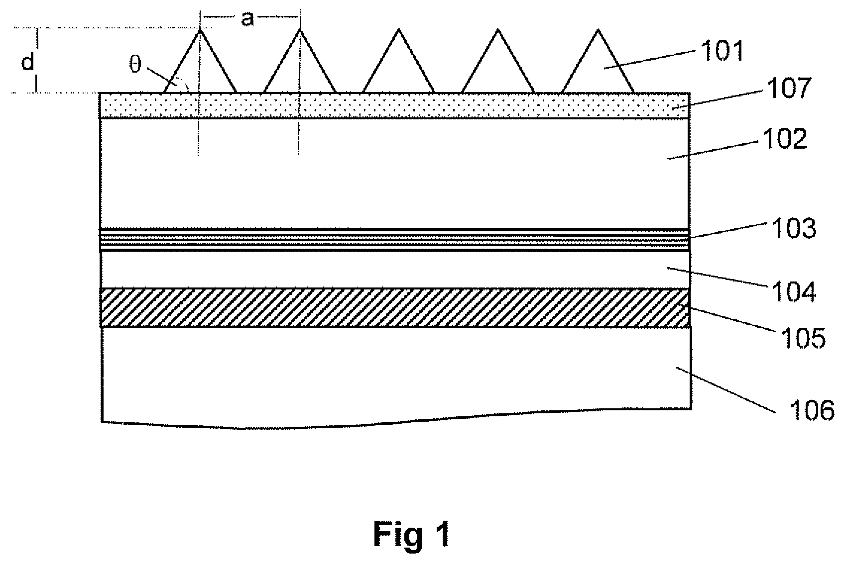
[0069]An aim of the present invention is to provide improved light extraction as well as tailored far-field emission from light emitting devices. These devices can employ a wide range of light emitting semiconductor material system including, but not restricted to, InGaN, InGaP, InGaAs, InP, or ZnO. The description will focus on the implementation of the directional light extraction technique implemented in green InGaN light emitting devices. However, the design can be equally optimised and implemented for other emission wavelengths (such as blue or UV) using this material as well as for other material systems, such as InGaP which is suitable for red and yellow wavelengths.

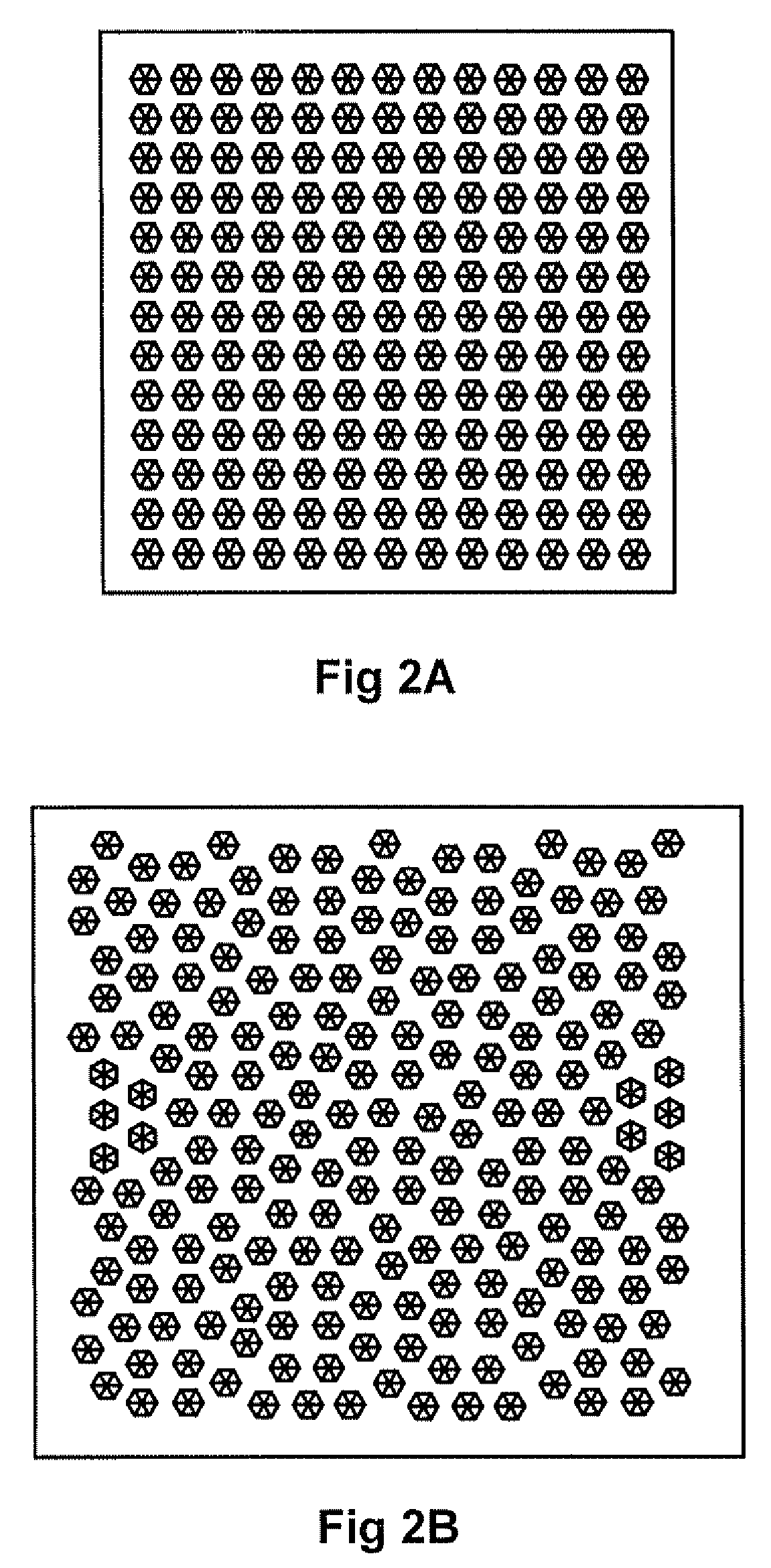
[0070]In a preferred implementation of the invention a novel high-order pyramidal photonic crystal (PC) or quasicrystal pattern is proposed that provides increased light extraction, as compared to first-order photonic crystal patterns. The PC design also allows for the tailoring of the far-field light distribution...


PUM


Abstract

A light-emitting device (LED) is described which exhibits high extraction efficiency and an emission profile which is substantially more directional than from a Lambertian source. The device comprises a light generating layer disposed between first and second layers of semiconductor material, each having a different type of doping. An upper surface of the first layer has a tiling arrangement of pyramidal or frustro-pyramidal protrusions of semiconductor material surrounded by a material of different refractive index which together comprise a photonic band structure. The protrusions and their tiling arrangement are configured for efficient extraction of light from the device via the upper surface of the first layer and in a beam that is substantially more directional than from a Lambertian source An enhanced device employs a reflector beneath the second layer to utilize the microcavity effect. A method for fabricating the device is also described which employs anisotropic wet etching to produce the pyramidal or frustro-pyramidal protrusions

Description

FIELD OF THE INVENTION[0001]The present invention relates to light-emitting diodes with improved light extraction and directionality, and in particular to devices employing photonic crystal structures.BACKGROUND OF THE INVENTION[0002]Light emitting diodes (LEDs) are based on a forward biased p-n junction and have recently reached sufficiently high brightness levels that they are now suitable for new solid-state lighting applications as well as replacements for projector light sources. Entry into these markets has also been enabled by the economical gains achieved through the high efficiencies of LEDs, as well as reliability, long lifetime and environmental benefits. In particular, applications in solid-state lighting require that LEDs exceed efficiencies currently achievable by alternative fluorescent lighting technologies.[0003]Back Light Units (BLU) for liquid crystal display (LCD) panels are key elements in the performance of an LCD panel. Currently, most LCD panels employ compac...

Claims


Application Information

Patent Timeline
Patent Type & Authority Patents(United States)
IPC IPC(8): H01L21/00H01L33/20
CPCH01L33/20H01L2933/0083
Inventor MCKENZIE, JAMESLEE, TOMZOOROB, MAJD
Owner QUANTUM NIL LTD
Why Eureka
Try Eureka