Shift register circuit and image display apparatus equipped with the same

a register circuit and image display technology, applied in logic circuits, digital storage, instruments, etc., can solve problems such as display defects, pixel rewriting, unnecessarily activating gate lines, etc., to reduce noise and suppress malfunction.

Active Publication Date: 2009-12-22
TRIVALE TECH
View PDF16 Cites 52 Cited by
  • Summary
  • Abstract
  • Description
  • Claims
  • Application Information

AI Technical Summary

Benefits of technology

[0028]The first aim of the present invention is to suppress malfunction caused by the leakage current of the constituting transistor in the bi-directional unit shift register. The second aim is to provide a bi-directional shift register in which input of the end pulse is not necessary. Furthermore, the third aim is to reduce the influence of noise added to the output terminal in the bi-directional unit shift register.
[0030]The transistor Q5 is turned ON and the first node is discharged when the first transistor is turned OFF and the second transistor is turned ON, and thus the first node is maintained at L level even if leakage current is generated at the third and fourth transistors, and malfunction caused by the leakage current is prevented.
[0034]The third and fourth nodes are charged when the output terminal is activated. When the output terminal is activated, the first node is boosted by the coupling via parasitic capacity of the first transistor, but the generation of leakage current of the third and fourth transistors is suppressed since the third and fourth nodes are being charged. Therefore, the potential of the first node is prevented from falling by the leakage current, whereby the problem of lowering in driving ability of the first transistor is resolved.
[0037]The final stage is inactivated by the output signal of the second dummy stage in the forward shift of shifting the signal from the previous stage to the subsequent stage, and the leading stage is inactivated by the output signal of the first dummy stage in the reverse shift of shifting the signal from subsequent stage to previous stage. That is, the output signal of the second dummy stage functions as end pulse in the forward shift, and the output signal of the first dummy stage function as end pulse in the reverse shift. Therefore, the end pulse does not need to be externally input for driving the shift register circuit. That is, the operation of the bi-directional shift is performed using the drive controlling device that does not include an end pulse generation circuit, whereby cost is reduced.

Problems solved by technology

When the potential of the first node rises by the leakage current and the clock signal, the problem of malfunction arises in which the first transistor that is to be turned OFF is turned ON, and the gate line is unnecessarily activated when the voltage between the gate and the source of the first transistor exceeds a threshold voltage.
When a pixel switch element (active transistor) arranged on each pixel is turned ON, the data in the pixel is re-written, and display defect occurs.
If the turning OFF of the pixel transistor is delayed, the data in the pixel may be re-written on the data of the next line, and display failure may occur.
Furthermore, it is not as simple as with shifting in only one direction since the output signal of the dummy stage may become the wrong start pulse when the shift direction is reversed, if the dummy stage is simply arranged.
Therefore, the drive controlling device of the gate line driving circuit for shifting the signal in bi-direction mounted with the output circuit of not only the start pulse but also of the end pulse is adopted, which increases the cost of the drive controlling device, that is, increases the cost of the display apparatus.
If the second transistor is not sufficiently turned ON in this case, the charges involved in the noise cannot be discharged from the output terminal, whereby the pixel transistor turns ON, and the wrong data may be written to the pixel.
However, since the relevant inverter is a ratio type inverter configured by the field effect transistors of the same conductivity type, the pass through current flowing through the inverter when the output of the inverter is at L level increases and the power consumption increases if the on-resistance of the transistor is lowered.

Method used


Image

  • Shift register circuit and image display apparatus equipped with the same
  • Shift register circuit and image display apparatus equipped with the same
  • Shift register circuit and image display apparatus equipped with the same

Examples


first embodiment

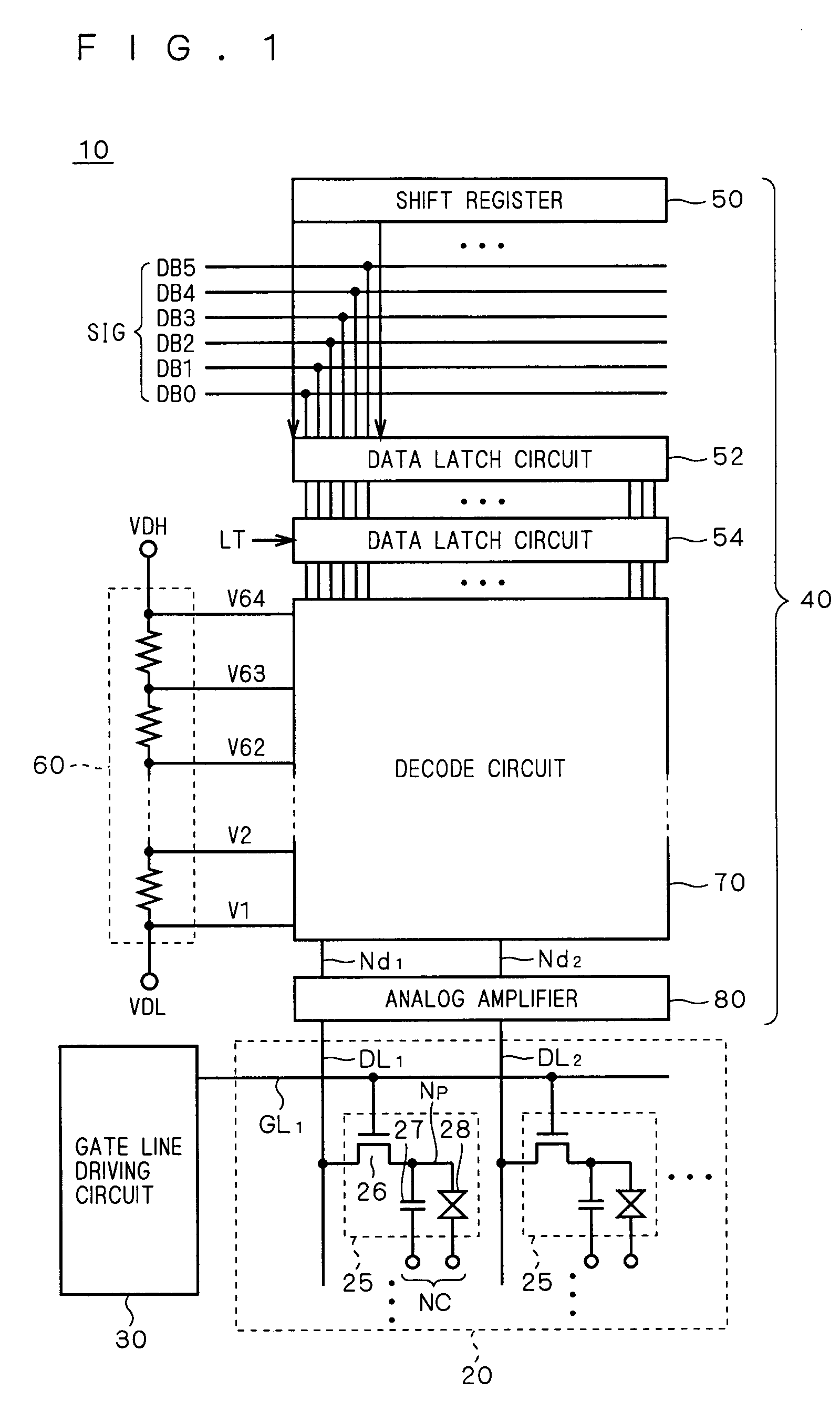
[0070]FIG. 1 is a schematic block diagram showing the configuration of a display apparatus according to a first embodiment of the present invention, showing the entire configuration of a liquid crystal display apparatus 10 as one example of the display apparatus.

[0071]The liquid crystal display apparatus 10 includes a liquid crystal array section 20, a gate line driving circuit (scanning line driving circuit) 30, and a source driver 40. As to be apparent from the description below, the bi-directional shift register according to the embodiment of the present invention is mounted on the gate line driving circuit 30, and is integrally formed with the liquid crystal array section 20.

[0072]The liquid crystal array section 20 includes a plurality of pixels 25 arranged in a matrix form. The gate lines GL1, GL2, . . . (collectively referred to as “gate line GL”) are arranged on each row of pixels (hereinafter referred to also as “pixel line”), and the data lines DL1, DL2, . . . (collectivel...

second embodiment

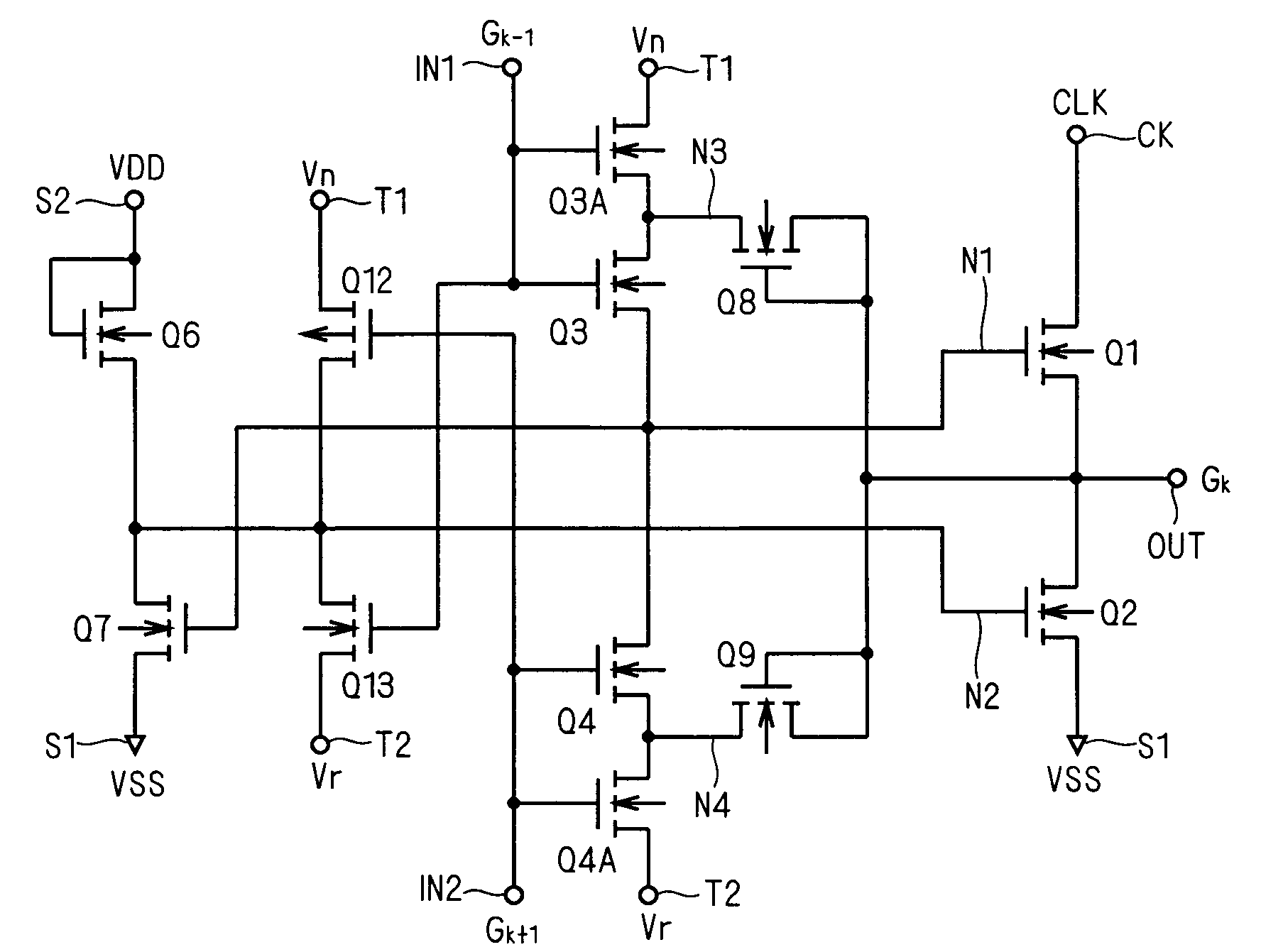
[0139]FIG. 9 is a circuit diagram of a bi-directional unit shift register SR according to the second embodiment. As shown in the figure, the unit shift register SR according to the present embodiment has a configuration in which a transistor Q12 and a transistor Q13 having a relatively large driving ability are additionally arranged with respect to the conventional circuit of FIG. 3.

[0140]The transistor Q12 is connected between the node N2 and the first voltage signal terminal T1, and the gate is connected to the second input terminal IN2. That is, the transistor Q12 functions to provide the first voltage signal Vn to the node N2 (second node) based on the signal (second input signal) input to the second input terminal IN2. The transistor Q13 is connected between the node N2 and the second voltage signal terminal T2, and the gate is connected to the first input terminal IN1. That is, the transistor Q13 functions to provide the second voltage signal Vr to the node N2 based on the sig...

third embodiment

[0149]FIG. 10 is a circuit diagram showing a configuration of a bi-directional unit shift register according to the third embodiment. As shown in the figure, the unit shift register SR according to the third embodiment has a configuration in which the transistor Q12 and the transistor Q13 having a relatively large driving ability shown in the second embodiment are additionally arranged with respect to the unit shift register SR (FIG. 7) of the first embodiment.

[0150]The circuit of FIG. 7 as described in the first embodiment operates to change the node N1 from L level to H level when the output signal Gk−1 of the previous stage is input to the first input terminal IN1 (time t1 in FIG. 8) in the operation of the forward shift, for example. However, such operation is performed from a state in which the transistor Q5 is turned ON, and thus the level of the node N1 is unlikely to rise. Therefore, the rising speed of the level of the node N1 may be slow, which inhibits the operation from ...


PUM


Abstract

Malfunction caused by leakage current of the transistor is prevented in the shift register in which the signal can be shifted bi-directionally. The bi-directional unit shift register includes a transistor Q1 between a clock terminal CK and an output terminal OUT, a transistor Q2 for discharging the output terminal OUT, and transistors Q3, Q4 for providing first and second voltage signals Vn, Vr, which are complementary to each other, to the first node or a gate node of the transistor Q1. Furthermore, a transistor Q5, having a gate connected to a second node or a gate node of the transistor Q2, for discharging the first node is arranged.

Description

BACKGROUND OF THE INVENTION[0001]1. Field of the Invention[0002]The present invention relates to shift register circuits configured only by field effect transistors of the same conductivity type used in scanning line driving circuit and the like of the image display apparatus etc., in particular, to a bi-directional shift register in which the direction of shifting the signal can be reversed.[0003]2. Description of the Background Art[0004]In the image display apparatus (hereinafter referred to as “display apparatus”), such as a liquid crystal display apparatus, a gate line (scanning line) is arranged for each pixel row (pixel line) of a display panel in which a plurality of pixels are arrayed in a matrix form, and the gate line is sequentially selected and driven at a cycle of one horizontal period of the display signal to update the displayed image. A shift register for performing the shift operation that completes the round in one frame period of the display signal is used for the...

Claims


Application Information

Patent Timeline
Patent Type & Authority Patents(United States)
IPC IPC(8): G11C19/00
CPCG11C19/28G09G3/20G09G3/36H03K19/00
Inventor TOBITA, YOUICHI
Owner TRIVALE TECH
Why Eureka
Try Eureka