Semiconductor device with buried conductive layer

a technology of conductive layer and semiconductor device, which is applied in the direction of semiconductor device, transistor, electrical apparatus, etc., can solve the problems of reducing channel length, affecting low-voltage operation of transistor, and deteriorating drain of transistor miniaturization, so as to reduce parasitic capacitance between backgate electrode and substrate, improve threshold controllability, and reduce parasitic capacitance

Inactive Publication Date: 2009-12-29
SEIKO EPSON CORP
View PDF25 Cites 4 Cited by
  • Summary
  • Abstract
  • Description
  • Claims
  • Application Information

AI Technical Summary

Benefits of technology

[0015]Accordingly, an advantage of the present invention is to provide a semiconductor device capable of improving threshold controllability by using a backgate electrode and reducing parasitic capacitance between the backgate electrode and source and drain layers, as well as to provide a method for manufacturing the semiconductor device.
[0016]In view of the problems described above, a semiconductor device according to a first aspect of the invention includes a first insulator formed at a part under a semiconductor layer, a second insulator formed under the semiconductor layer in an arranged manner avoiding the first insulator and having a relative dielectric constant different from that of the first insulator, a backgate electrode formed under the first and second insulators, a gate electrode formed on the semiconductor layer, and a source layer and a drain layer formed in the semiconductor layer to be respectively arranged on opposite lateral sides of the gate electrode.
[0017]In this manner, the backgate electrode can be arranged under the gate electrode and can also be coupled to a channel region via a high-dielectric material. Furthermore, the backgate electrode can be coupled to the source and drain layers via a low dielectric material. Consequently, parasitic capacitance between the backgate electrode and the substrate can be reduced while increasing coupling capacitance between the backgate electrode and the channel region. Accordingly, without restriction by arrangements of the gate electrode, source and drain contacts, etc., the backgate electrode can be arranged and also threshold controllability by the backgate electrode can be improved. As a result, transistor operating and standby power consumption can be reduced and high-speed performance of the SOI transistor can be achieved.
[0018]In addition, the semiconductor device according to the first aspect of the invention may further include a wiring layer for connecting the backgate electrode to the gate electrode.
[0019]In this manner, control can be performed such that the backgate electrode has the same potential as that of the gate electrode, thereby enhancing controllability to the potential of a deep part in the channel region. Accordingly, while suppressing an increase in chip size, an off-time leakage current and also operating and standby power consumption can be reduced. Moreover, the field-effect transistor can have a high breakdown voltage.
[0020]In addition, a semiconductor device according to a second aspect of the invention includes a semiconductor layer arranged on a semiconductor substrate to be film-formed by epitaxial growth, a first buried insulator buried in a part between the semiconductor substrate and the semiconductor layer, a second buried insulator buried between the semiconductor substrate and the semiconductor layer in an arranged manner avoiding the first buried insulator and having a relative dielectric constant different from that of the first buried insulator, a gate electrode formed on the semiconductor layer, and a source layer and a drain layer formed in the semiconductor layer to be respectively arranged on opposite lateral sides of the gate electrode.

Problems solved by technology

In previous semiconductor integrated circuits, however, reduction in channel length due to transistor miniaturization deteriorates drain-current rising characteristics in a subthreshold region.
This hinders low-voltage operation of a transistor, and increases leakage current during an off-time period thereof and its operating and standby power consumption.
Moreover, the deterioration even leads to destruction of the transistor.
Furthermore, there is a problem that arrangement of a backgate electrode on an entire surface region under a field-effect transistor increases parasitic capacitance between the backgate electrode and source and drain layers, thereby hindering high-speed performance of the SOI transistor.
Moreover, the field-effect transistor can have a high breakdown voltage.

Method used


Image

  • Semiconductor device with buried conductive layer
  • Semiconductor device with buried conductive layer
  • Semiconductor device with buried conductive layer

Examples


first embodiment

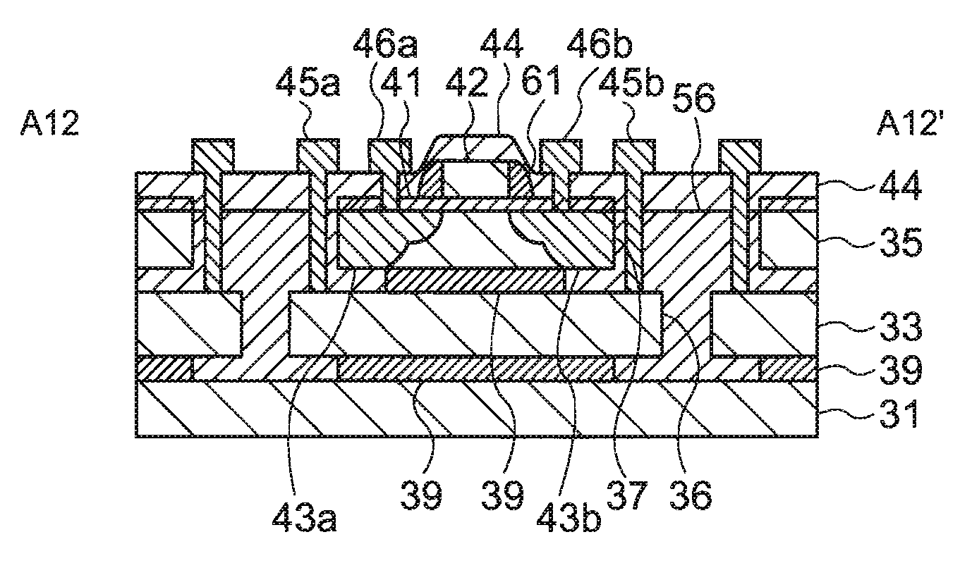
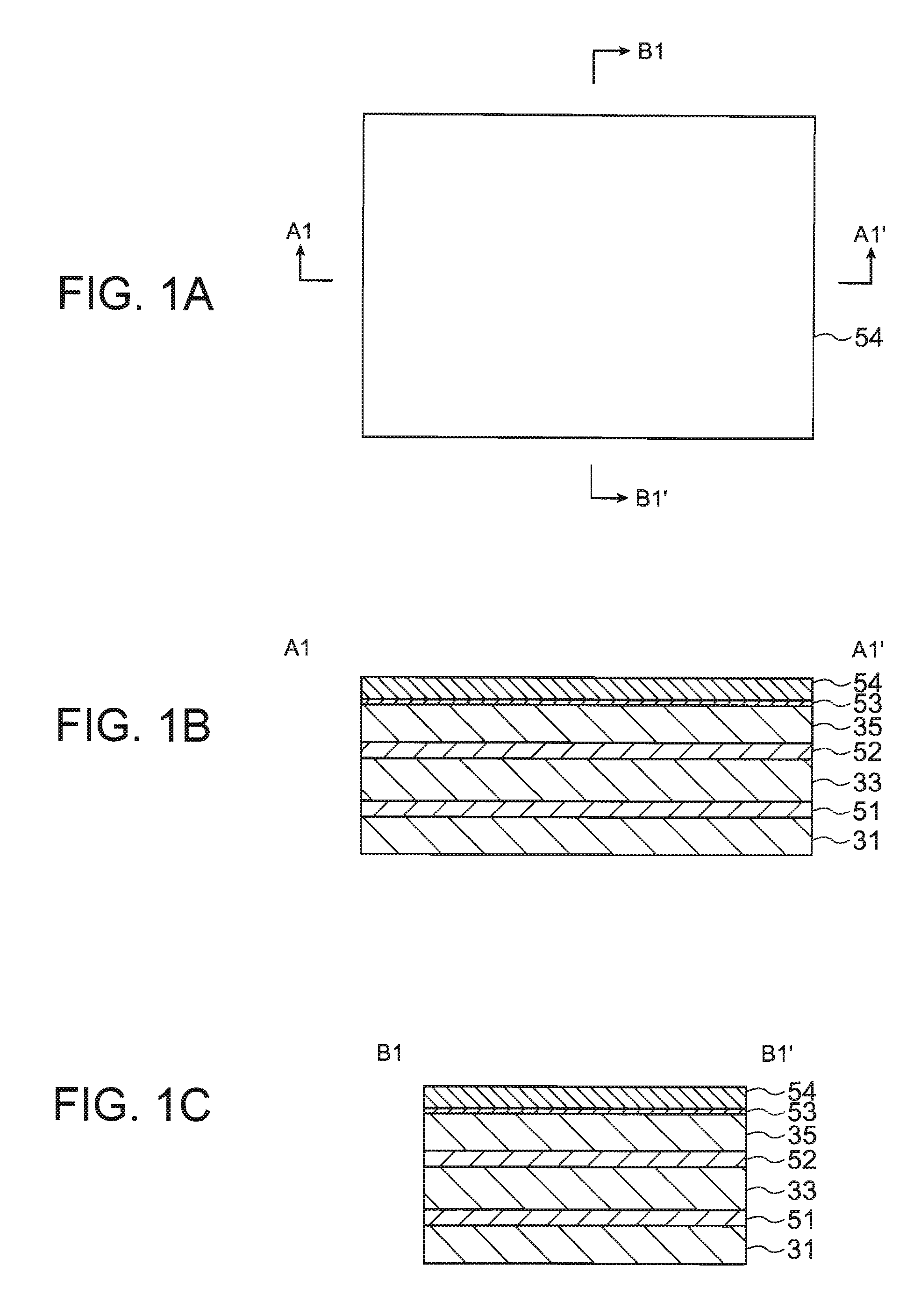
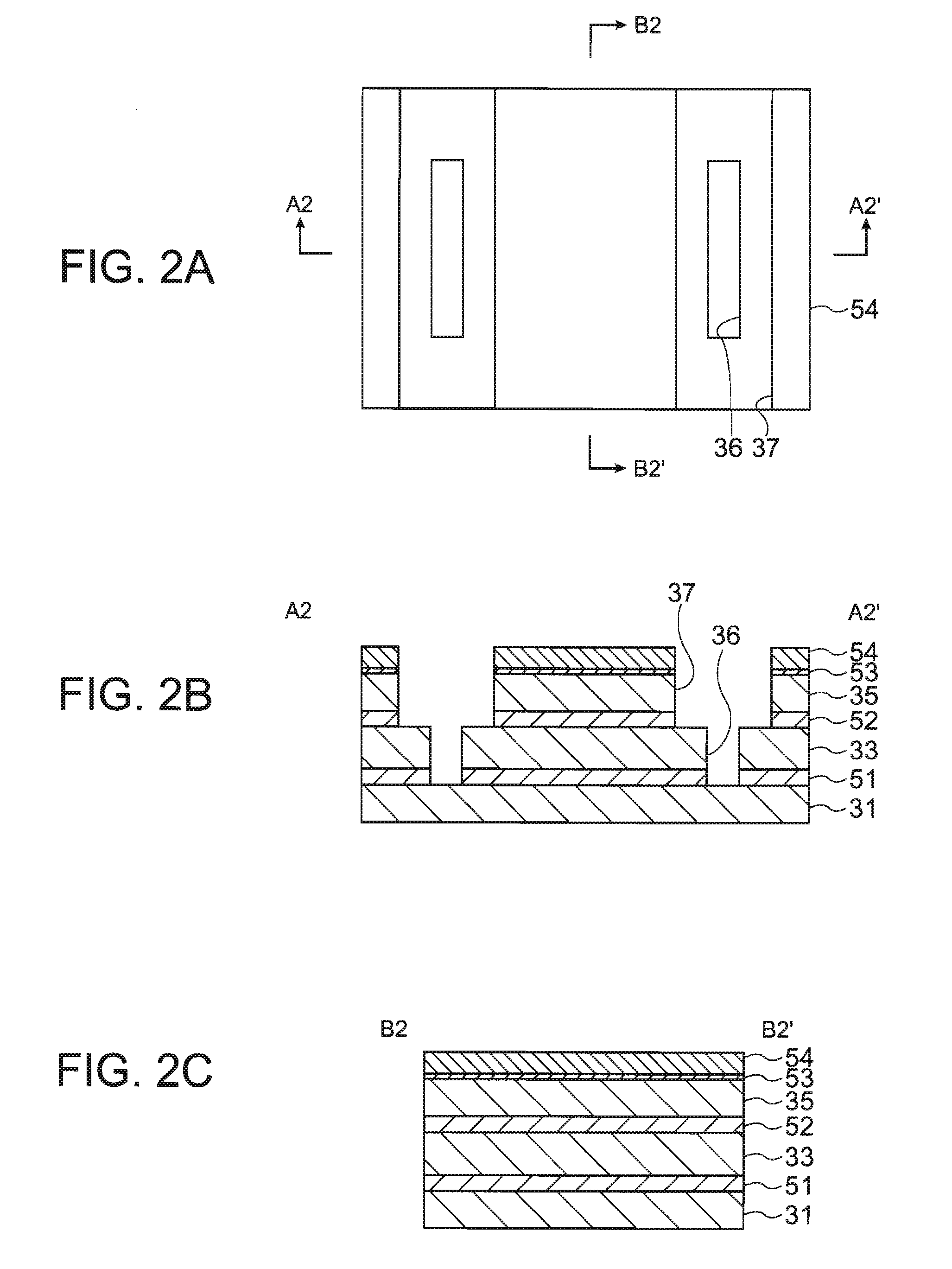
[0093]FIGS. 1A, 2A, 3A, 4A, 5A, 6A, 7A, 8A, 9A, 10A, 11A and 12A are plan views showing a method for manufacturing a semiconductor device according to a first embodiment of the invention. FIGS. 1B, 2B, 3B, 4B, 5B, 6B, 7B, 8B, 9B, 10B, 11B and 12B are sectional views taken along lines A1-A1′, A2-A2′, A3-A3′, A4-A4′, A5-A5′, A6-A6′, A7-A7′, A8-A8′, A9-A9′, A10-A10′, A11-A11′ and A12-A12′, respectively, as shown in the above-mentioned figures. FIGS. 1C, 2C, 3C, 4C, 5C, 6C, 7C, 8C, 9C, 10C, 11C and 12C are sectional views taken along lines B1-B1′, B2-B2′, B3-B3′, B4-B4′, B5-B5′, B6-B6′, B7-B7′, B8-B8′, B9-B9′, B10-B10′, B11-B11′ and B12-B12′, respectively, as shown in the above-mentioned figures.

[0094]In FIGS. 1A to 1C, semiconductor layers 51, 33, 52 and 35 are sequentially laminated in this order on a semiconductor substrate 31. The semiconductor layers 51 and 52 may be made of material having an etching rate greater than that of the semiconductor substrate 31 and the semiconductor la...

second embodiment

[0114]FIGS. 13A, 14A, 15A, 16A, 17A, 18A, 19A, 20A, 21A, 22A, 23A, 24A, 25A and 26A are plan views showing a method for manufacturing a semiconductor device according to a second embodiment of the invention. FIGS. 13B, 14B, 15B, 16B, 17B, 18B, 19B, 20B, 21B, 22B, 23B, 24B, 25B and 26B are sectional views taken along lines A13-A13′, A14-A14′, A15-A15′, A16-A16′, A17-A17′, A18-A18′, A19-A19′, A20-A20′, A21-A21′, A22-A22′, A23-A23′, A24-A24′, A25-A25′ and A26-A26′, respectively, as shown in the above-mentioned figures. FIGS. 13C, 14C, 15C, 16C, 17C, 18C, 19C, 20C, 21C, 22C, 23C, 24C, 25C and 26C are sectional views taken along lines B13-B13′, B14-B14′, B15-B15′, B16-B16′, B17-B17′, B18-B18′, B19-B19′, B20-B20′, B21-B21′, B22-B22′, B23-B23′, B24-B24′, B25-B25′ and B26-B26′ respectively, as shown in the above figures.

[0115]In FIGS. 13A to 13C, a first semiconductor layer 2 is formed on a semiconductor substrate 1 by epitaxial growth, and a second semiconductor layer 3 is formed on the fi...


PUM


Abstract

A semiconductor device includes a first insulator formed at a part under a semiconductor layer, a second insulator formed under the semiconductor layer in an arranged manner avoiding the first insulator and having a relative dielectric constant different from that of the first insulator, a backgate electrode formed under the first and second insulators, a gate electrode formed on the semiconductor layer, and a source layer and a drain layer formed in the semiconductor layer to be respectively arranged on opposite lateral sides of the gate electrode.

Description

BACKGROUND[0001]1. Technical Field[0002]The present invention relates to a semiconductor device and a method for manufacturing the same. In particular, the invention is suitably applied to a method for forming a field-effect transistor having a backgate electrode.[0003]2. Related Art[0004]Much attention is given to the usefulness of a field-effect transistor formed on a silicon-on-insulator (SOI) substrate due to the easiness of device separation, latch-up free operation, a small amount of source and drain junction capacitance and the like. In particular, a fully-depleted SOI transistor can exhibit low power consumption and high-speed performance, while operating at low voltage. Accordingly, research has been actively conducted to develop SOI transistors operating in a fully-depleted mode. In this case, an SOI substrate is formed of, for example, a separation by implanted oxygen (SIMOX) substrate, a bonding substrate or the like, as disclosed in first and second patent examples of r...

Claims


Application Information

Patent Timeline
Patent Type & Authority Patents(United States)
IPC IPC(8): H01L29/786
CPCH01L29/6675H01L29/78648H01L29/66772H01L27/12H01L21/18
Inventor KATO, JURI
Owner SEIKO EPSON CORP
Why Eureka
Try Eureka