ESD protection structure

a protection structure and electrostatic discharge technology, applied in the direction of semiconductor devices, semiconductor/solid-state device details, electrical apparatus, etc., can solve the problems of slowing down the propagation of input signals, inability to tolerate high-speed input functions, and vulnerable cmos input buffers to esd damage, etc., to achieve the effect of reducing input capacitan

Inactive Publication Date: 2009-12-29
ALTERA CORP
View PDF18 Cites 7 Cited by
  • Summary
  • Abstract
  • Description
  • Claims
  • Application Information

AI Technical Summary

Benefits of technology

[0008]The present invention is a novel ESD structure for protecting an integrated circuit from ESD damage. In one embodiment, the structure comprises, in part, a NMOS transistor having a source and drain in a well in a substrate and a gate on the substrate with the drain and source being connected between a series diode and ground, and the gate being connected to ground. The anode and the cathode of the series diode are connected to the input pad and the drain of the NMOS transistor, respectively. The series diode serves to reduce the input capacitance imposed by the large NMOS transistor. The structure further comprises another diode having a cathode connected to the input pad and an anode connected to the well so that the diode is reverse-biased in the event of a positive voltage ESD event on the input p

Problems solved by technology

For example, gates in N-type metal metal-oxide-silicon (NMOS) and P-type metal-oxide-silicon (PMOS) transistors in input buffers of a CMOS IC are often directly connected to input pads of the IC, causing the CMOS input buffers to be vulnerable to ESD damage.
Large ESD devices are used to protect the gates of a CMOS input buffer, but the large ESD devices add significant capacitance to the input pins, and this slows down the input signal propagation.
This is not tolerable for high-speed input functions, such as high-speed clock inputs.
One problem with a grounded-gate NMOS transistor is large capacitance between its drain and ground due to large transistor s

Method used


Image

  • ESD protection structure
  • ESD protection structure
  • ESD protection structure

Examples


Embodiment Construction

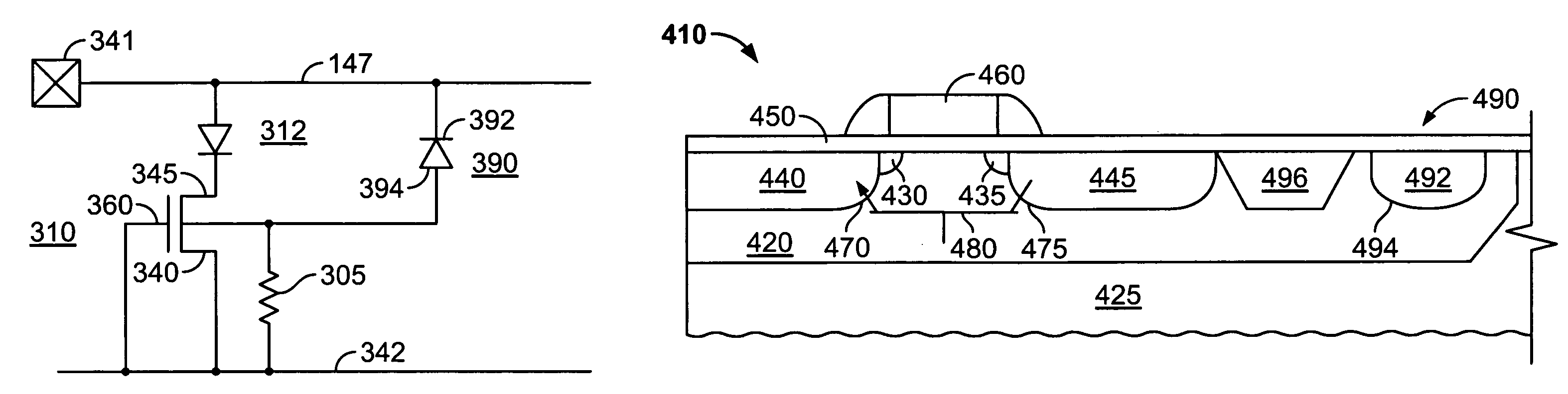
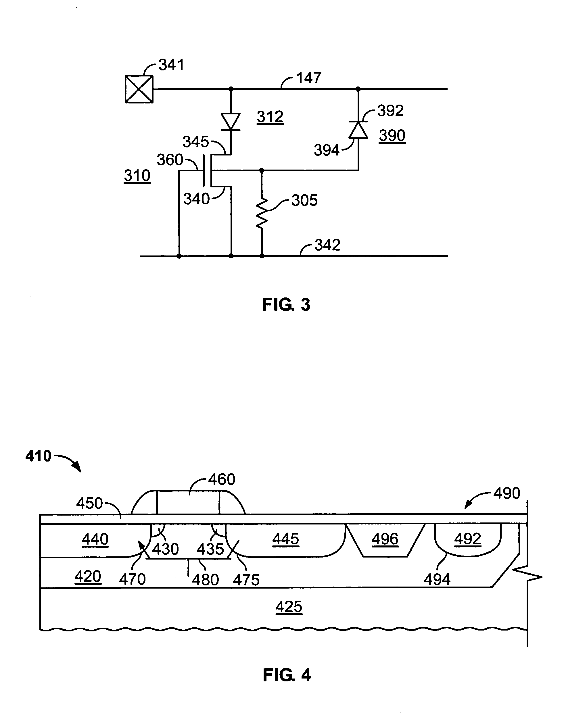
[0016]In accordance with the present invention, a diode is connected between the substrate of the MOS transistor and the input pad and is connected so that the diode is reverse-biased in the event of a positive voltage ESD event on the input pad. As a result, in a positive voltage ESD event, the avalanche effect in the diode rapidly injects current into the substrate and therefore into the base of the parasitic lateral bipolar transistor in the MOS transistor so as to trigger the transistor into conduction and discharge the ESD pulse. In the event of a negative voltage ESD event on the input pad, the diode is forward-biased and conducts in the forward direction to discharge the ESD pulse through the well / substrate of the NMOS transistor.

[0017]A circuit schematic of an illustrative embodiment of the invention is set forth in FIG. 3. As shown therein, the circuit comprises an NMOS transistor 310 and a diode 390. NMOS transistor 310 comprises a source 340, a drain 345 and a gate 360. T...


PUM


Abstract

An ESD protection structure includes, in part, a NMOS transistor having a source and drain in a well in a substrate and a gate on the substrate with the source and drain being connected between ground and a series diode, and the gate being connected to ground. The structure further includes a diode having a cathode connected to the input pad and an anode connected to the well so that the diode is reverse-biased in the event of a positive voltage ESD event on the input pad. As a result, in a positive voltage ESD event, the avalanche effect rapidly injects current into the substrate and therefore into the base of the parasitic bipolar transistor so as to trigger the transistor into conduction and discharge the ESD pulse. Alternatively, the diode is a Zener diode and the current is generated by the Zener effect. A complementary structure provides protection against a negative ESD pulse.

Description

CROSS-REFERENCE TO RELATED APPLICATIONS[0001]This application is a continuation-in-part of application Ser. No. 10 / 882,874, filed Jun. 30, 2004 now U.S. Pat. No. 7,195,958 for “Methods of Fabricating ESD Protection Structures,” which application is a divisional of application Ser. No. 10 / 298,104, filed Nov. 14, 2002, now U.S. Pat. No. 6,777,721, for “SCR Device for ESD Protection.” The '874 application and the '721 patent are incorporated by reference herein in their entireties.FIELD OF THE INVENTION[0002]This relates to electrostatic discharge (ESD) protection structures for protecting an integrated circuit from ESD damage.BACKGROUND OF THE INVENTION[0003]ESD protection has been a main concern in the reliability of integrated circuit (IC) products in submicron complimentary metal-oxide-silicon (CMOS) technologies. For example, gates in N-type metal metal-oxide-silicon (NMOS) and P-type metal-oxide-silicon (PMOS) transistors in input buffers of a CMOS IC are often directly connected...

Claims


Application Information

Patent Timeline
IPC IPC(8): H01L23/62H01L29/72H01L29/73H01L29/74H01L31/111
CPCH01L27/0259
Inventor O, HUGH SUNGKISHIH, CHIH-CHINGHUANG, CHENG-HSIUNGLIU, YOW-JUANG BILL
Owner ALTERA CORP
Why Eureka
Try Eureka