Circuit board structure with embedded electronic components

a technology of electronic components and circuit boards, applied in the association of printed circuit non-printed electric components, fixed capacitor details, lighting and heating apparatus, etc., can solve the problems of unfit ceramics for large-scale thin-film fabrication, rare thin-film ceramics, etc., and achieve the effect of enhancing the bending strength of the circuit board structur

Active Publication Date: 2009-12-29
PHOENIX PRECISION TECH CORP
View PDF11 Cites 119 Cited by
  • Summary
  • Abstract
  • Description
  • Claims
  • Application Information

AI Technical Summary

Benefits of technology

[0006]In light of the aforesaid drawbacks of the prior art, it is a primary objective of the present invention to provide a circuit board structure with embedded electronic components, that allows the bending strength of the circuit board structure to be enhanced.
[0007]Another objective of the present invention is to provide a circuit board structure with embedded electronic components, that makes the circuit board structure structurally simpler.
[0013]Accordingly, a circuit board structure with embedded electronic components disclosed in the present invention is structurally reinforced by the metal layers and metal oxide layers of the carrier board so as to enhance the bending strength of the circuit board structure during subsequent processes. Regarding the carrier board of the present invention, the second metal layer is formed with a high dielectric material layer and an electrode board. It allows the high dielectric material layer, the electrode board and the second metal layer, to form a capacitance component. Therefore, the present invention overcomes various drawbacks of using a ceramic substrate as a carrier board as disclosed in the prior art.

Problems solved by technology

However, owing to their brittleness and low bending strength, ceramic substrates rarely come in thin, large sizes and thereby are limited in use to small modules or packages.
Accordingly, an issue facing the semiconductor manufacturers and calling for urgent solution involves developing a circuit board structure with embedded electronic components and a fabrication method thereof with a view to solving drawbacks of the prior art as follows: first, a circuit board structure with a ceramic substrate functioning as a carrier element for a semiconductor chip has low bending strength; second, ceramic is unfit for fabrication of large, thin substrates; and third, the prior art does not disclose a method for forming capacitance components in a circuit board directly, which could be more efficient.

Method used


Image

  • Circuit board structure with embedded electronic components
  • Circuit board structure with embedded electronic components
  • Circuit board structure with embedded electronic components

Examples


first embodiment

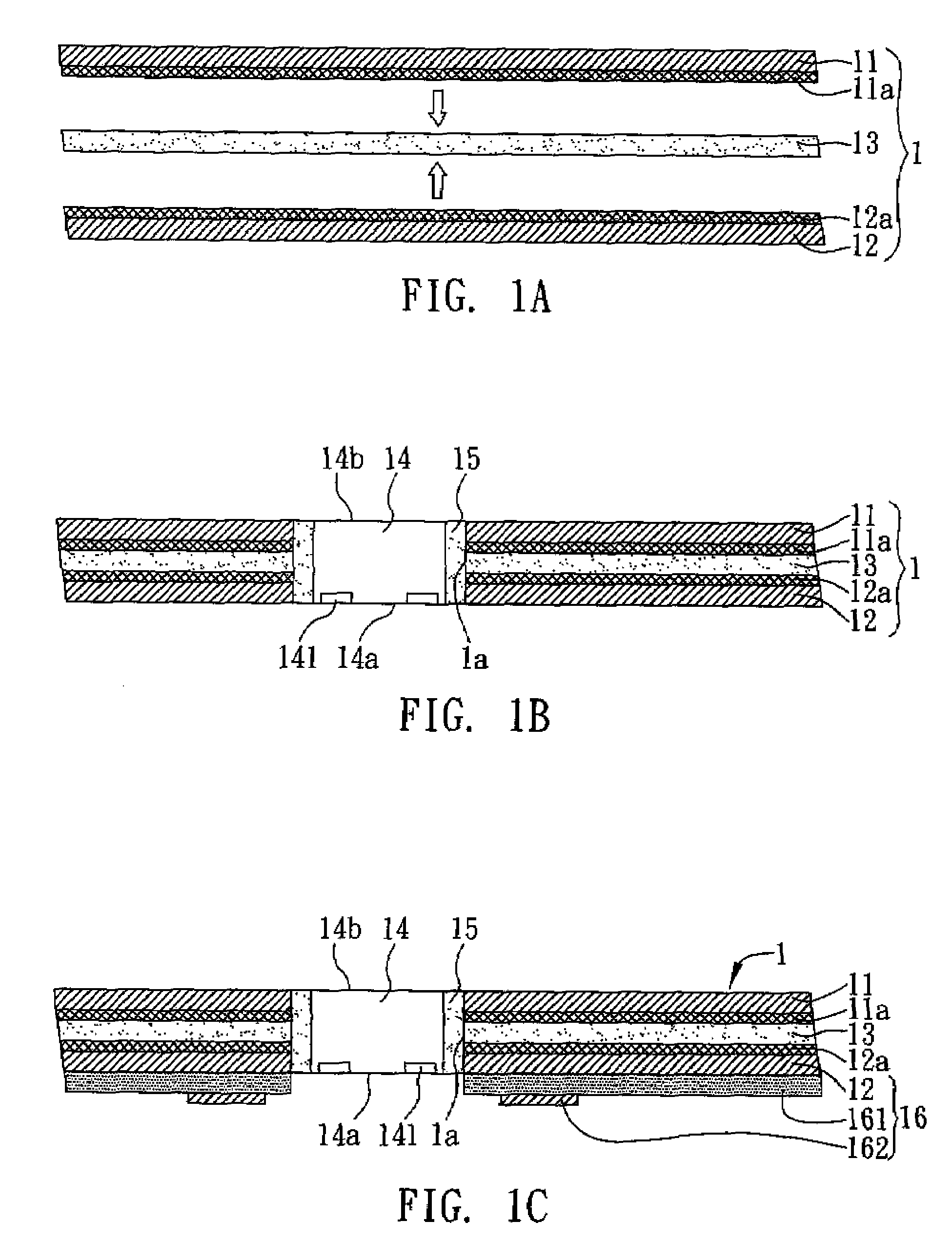
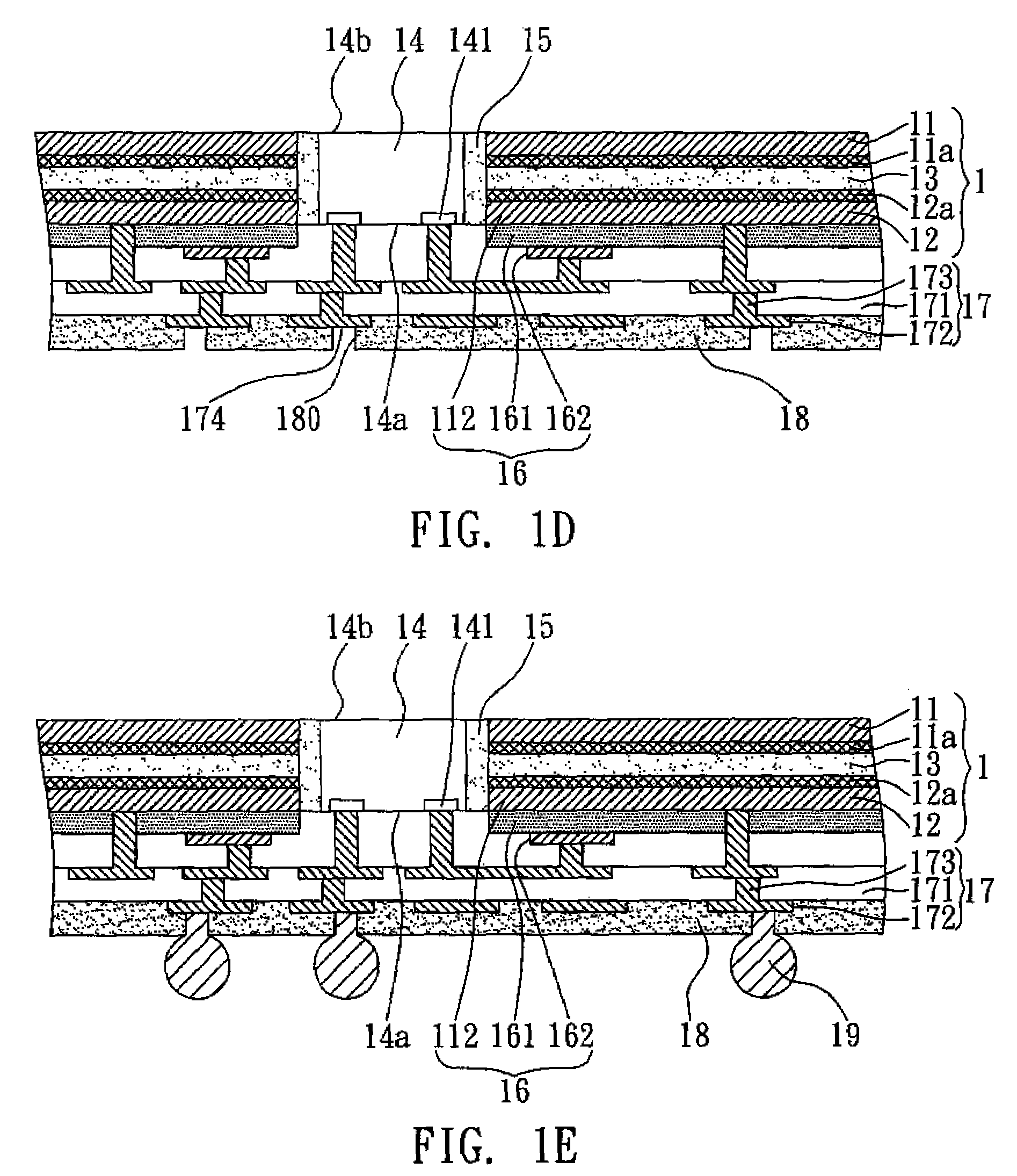
[0018]FIGS. 1A to 1E are cross-sectional views showing an embodiment of a method for fabricating a circuit board structure with embedded electronic components of the present invention.

[0019]As shown in FIG. 1A, the method comprises: providing a first metal layer 11 and a second metal layer 12, wherein the first and second metal layers 11 and 12 comprise aluminum; performing an oxidation process on the first and second metal layers 11 and 12 so as to form a first metal oxide layer l a and a second metal oxide layer 12a, such as aluminum oxide, on the first and second metal layers 11 and 12, wherein the first and second metal oxide layers 11a and 12a are formed on one of the surfaces of the first and second metal layers 11 and 12 either by oxidizing both of the surfaces of the first and second metal layers 11 and 12 and then removing one metal oxide layer from one surface of each of the oxidized metal layers by etching, or by performing the oxidation process after forming a release fi...

second embodiment

[0031]FIG. 2 is a cross-sectional view showing the second embodiment of a circuit board structure with embedded electronic components of the present invention.

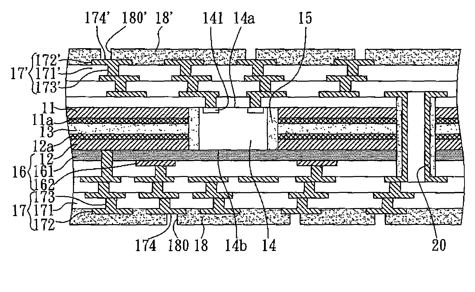
[0032]In this embodiment, in addition to the circuit build-up structure 17, another circuit build-up structure 17′ is formed on the non-active surface 14b of the semiconductor chip 14 and the first metal layer 11, and, additionally, the carrier board 1 is formed with and penetrated by at least one plated through hole 20. The plated through hole 20 electrically connects the circuit build-up structures 17 and 17′ so as to enhance the electrical function of the circuit board structure.

third embodiment

[0033]FIG. 3 is a cross-sectional view showing the third embodiment of a circuit board structure with embedded electronic components of the present invention.

[0034]This embodiment differs from the second embodiment in that the active surface of the semiconductor chip faces in the same direction as the first metal layer faces instead of the second metal layer.

[0035]As shown in FIG. 3, the circuit build-up structure 17 is formed on the surfaces of the non-active surface 14b of the semiconductor chip 14 and the high dielectric material layer 161 and electrode board 162 of the capacitance component 16. The circuit build-up structure 17 is formed with the conductive structures 173 for electrical connection with the electrode board 162 of the capacitance component 16. Another circuit build-up structure 17′ is formed on the active surface 14a of the semiconductor chip 14 and the first metal layer 11. The circuit build-up structure 17′ is formed with conductive structures 173′ for electrica...


PUM


Abstract

A circuit board structure with embedded electronic components includes: a carrier board having an adhesive layer with two surfaces formed with first and second metal oxide layers covered by first and second metal layers and having at least one through hole; at least one semiconductor chip received in the through hole of the carrier board; an adhesive material filling a gap between the through hole and the semiconductor chip so as to secure the semiconductor chip in position to the through hole; a high dielectric material layer formed outwardly on the second metal layer; and at least one electrode board formed outwardly on the high dielectric material layer such that a capacitance component is formed with the second metal layer, high dielectric material layer, and electrode board. Accordingly, the capacitance component is integrated into the circuit board structure.

Description

BACKGROUND OF THE INVENTION[0001]1. Field of the Invention[0002]The present invention relates to circuit board structures with embedded electronic components, and more particularly, to a circuit board structure integrated with a capacitance component and a semiconductor chip.[0003]2. Description of the Prior Art[0004]Electronic products nowadays are becoming lighter, thinner and smaller, thus making the semiconductor industry embed electronic components into package substrates so as to conform with the trend of miniaturization. For instance, most semiconductor manufacturers perform a process that involves embedding active components (e.g., semiconductor chips) and passive components (e.g., resistors, capacitors, and inductors) in an alumina ceramic substrate, for example, and then patterning a circuit on the ceramic substrate so as to form a circuit board structure having active / passive component embedded therein. However, owing to their brittleness and low bending strength, ceramic...

Claims


Application Information

Patent Timeline
Patent Type & Authority Patents(United States)
IPC IPC(8): F23Q3/00
CPCH01L24/19H01L23/5389H01L24/24H01L24/82H05K1/185H05K3/4608H05K3/4641H01L23/49816H01L2224/24227H01L2924/01013H01L2924/01057H01L2924/18162H01L2924/19041H01L2924/19042H01L2924/19043H01L2924/30105H05K1/162H05K3/429H05K3/445H05K2201/09309H05K2201/09536H05K2201/10674H05K2203/0315H01L2924/01033H01L2924/014H01L23/49827H01L2924/15787H01L2924/00
Inventor HSU, SHIH-PINGCHIA, KAN-JUNG
Owner PHOENIX PRECISION TECH CORP
Why Eureka
Try Eureka