

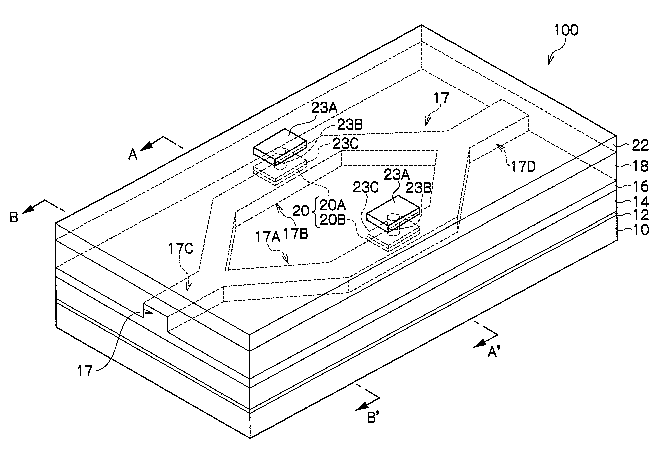
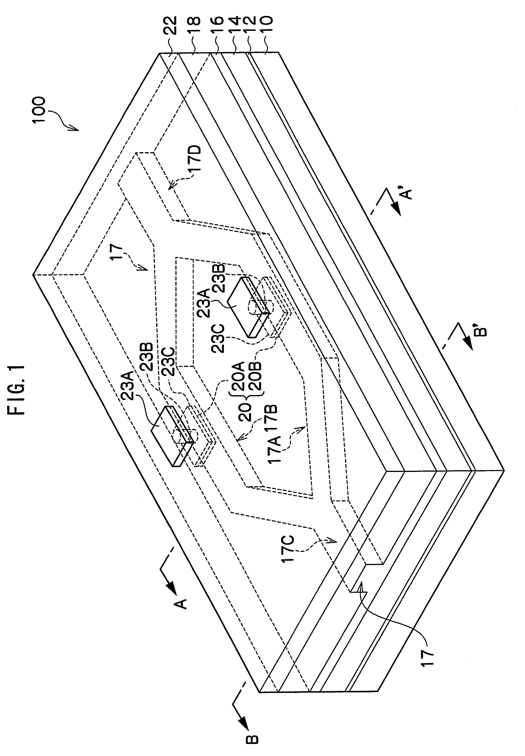
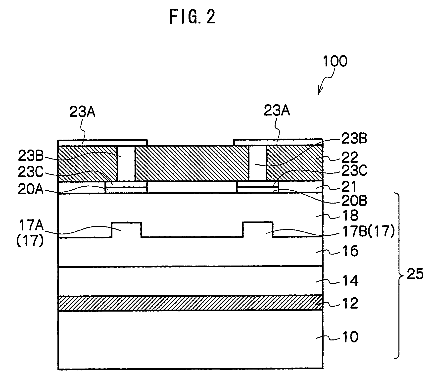
Optical waveguide element
a waveguide and element technology, applied in the field of optical waveguide elements, can solve the problems of slow response speed, high manufacturing cost, and limited frequency region to which the element may be applied
- Summary
- Abstract
- Description
- Claims
- Application Information
AI Technical Summary
Benefits of technology
Problems solved by technology
Method used
Image

Examples
example 1
[0112]First, a solution including 77 parts by mass of cyclohexanone, 9 parts by mass of tetrahydrofuran, 10 parts by mass of polysulfone, and 4 parts by mass of Disperse Red 1 (trade name, manufactured by Tokyo Chemical Industry Co., Ltd.; hereinafter, may be referred to as DR1), assuming that the total mass of all of these materials (hereinafter, referred to as PS solution) is 100 parts by mass, is prepared as a solution of a non-linear optical material. The refractive index of a film formed from the material is measured by a prism coupling method and is confirmed to be 1.63.
[0113]Then, an Au layer having a thickness of 500 nm as a lower electrode is provided on a surface of a silicon substrate (diameter: 50.8 mm, thickness: 0.5 mm) by a sputtering method.
[0114]Then, an ultraviolet curable acrylic resin having a refractive index of 1.54 is applied as a lower cladding layer onto a lower electrode surface, and is irradiated with an ultraviolet ray, to form a cured resin film having a...
PUM
 Abstract
Description
Claims
Application Information