Semiconductor device and method of manufacturing thereof

a semiconductor and printed circuit board technology, applied in semiconductor devices, solid-state devices, basic electric elements, etc., can solve the problems of forming voids, affecting the quality of semiconductor chips, so as to reduce the warping of semiconductor chips and printed circuit boards, and reduce the effect of manufacturing efficiency

Active Publication Date: 2010-01-26
DOW TORAY CO LTD
View PDF12 Cites 15 Cited by
  • Summary
  • Abstract
  • Description
  • Claims
  • Application Information

AI Technical Summary

Benefits of technology

[0011]The method of the invention provides efficient manufacturing of sealed semiconductor devices, prevents formation of voids in the sealing material, allows precise control of thickness of the cured silicone bodies that seal the devices, protects the bonding wires from disconnection and undesired contact, and reduces warping of semiconductor chips and printed-circuit boards. In particular, the invention provides such a method of manufacturing sealed semiconductor devices that allows compression molding of a curable silicone composition at the relatively low temperature required for reducing warping of semiconductor chips and printed-circuit boards. Furthermore, the invention provides sealed semiconductor devices that possess the aforementioned properties.

Problems solved by technology

If a transfer-molding is employed in resin sealing of thin packages, the thickness of the sealing resin could be precisely controlled, whereas there are problems that vertical displacements of semiconductor chips occur in a flow of a liquid sealing resin, or breakage of wires and contact between the wires occur because of deformations of bonding wires connected to semiconductor chips under the effect of pressure in the flow of the liquid sealing resin.
On the other hand, although potting or screen-printing with a liquid sealing resin to some extent protects the bonding wires from breakage and mutual contact, these methods make accurate control of sealing-resin coatings more difficult and can easily lead to formation of voids.
However, due to thinning of semiconductor chips that occurs with miniaturization of semiconductor elements, these methods increase warping of the semiconductor chips and printed-circuit boards and may lead to damaging of semiconductor devices and to worsening of their performance characteristics.

Method used


Image

  • Semiconductor device and method of manufacturing thereof
  • Semiconductor device and method of manufacturing thereof
  • Semiconductor device and method of manufacturing thereof

Examples


example 1

Practical Example 1

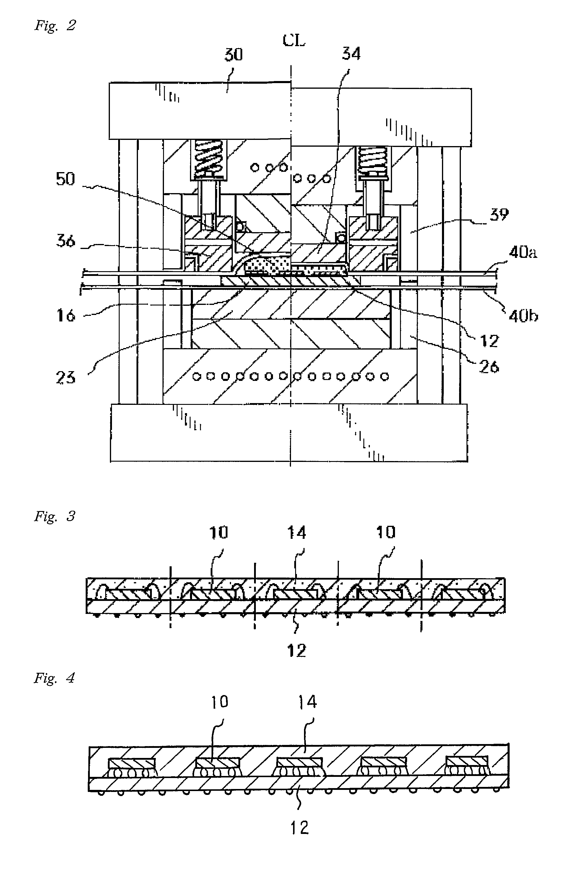
[0114]In the present practical example, a semiconductor device of the type shown in FIG. 3 was used. More specifically, (8 mm×14 mm) semiconductor chips were fixed to a (70 mm×160 mm) polyimide-resin printed-circuit board via a 35 μm-thick epoxy-resin die-bond agent layer. The printed-circuit board was comprised of a laminated structure formed by applying an 18 μm-thick copper foil via an epoxy-resin adhesive layer having a 17 μm thickness onto one side of a 75 μm-thick polyimide resin film. Circuit patterns were then made from the aforementioned foil. Portions required for wire bonding of the circuit patterns were removed, and the surface of the printed-circuit board was coated with a photosensitive solder mask. The circuit patterns and chip bumps of the semiconductor devices were electrically interconnected and wire bonded via 48 gold bonding wires. In total, 54 semiconductor chips divided into 3 blocks of 18 chips in each were secured to the printed-circuit boa...

example 2

Practical Example 2

[0116]A semiconductor device was prepared in the same manner as in Practical Example 1 with the exception that a silicone rubber composition (II) prepared by mixing in a 1:1 weight ratio the liquid A and the liquid B of a two-liquid type silicone rubber composition having components shown in Table 1 was used instead of the silicone rubber composition (I). Characteristics of the obtained semiconductor device are shown in Table 4.

[0117]

TABLE 1Example No.Practical Example 1Practical Example 2ComponentsIIISilicone Rubber CompositionLiquid ALiquid BLiquid ALiquid BCompositionOrganopolysiloxane (A-1)(parts by weight)5.763.03.3Organopolysiloxane (A-3)(parts by weight)——99Organopolysiloxane (A-4)(parts by weight)18.814 12.57.7Organopolysiloxane (B-1)(parts by weight)—3—3Platinum-type Catalyst (C-1)(ppm*)20—20—Filler (D-1)(parts by weight)6868 6868Filler (D-2)(parts by weight)77——Filler (D-3)(parts by weight)——77Adhesion Promoter(parts by weight)—2—2Pigment(parts by weight...

example 3

Practical Example 3

[0118]A semiconductor device was prepared in the same manner as in Practical Example 1 with the exception that a one-liquid type silicone rubber composition (III) having components shown in Table 2 was used instead of the silicone rubber composition (I) and that after compression molding for 4 minutes at 120° C. and a pressure of 50 kgf / cm2 the product was further heat treated in an oven for 1 hour at 120° C. Characteristics of the obtained semiconductor device are shown in Table 4.


PUM

PropertyMeasurementUnit
thicknessaaaaaaaaaa
viscosityaaaaaaaaaa
viscosityaaaaaaaaaa

Abstract

A method of manufacturing a semiconductor device sealed in a cured silicone body by placing a semiconductor device into a mold and subjecting a curable silicone composition that fills the spaces between said mold and said semiconductor device to compression molding, wherein the curable silicone composition comprises the following components: (A) an organopolysiloxane having at least two alkenyl groups per molecule; (B) an organopolysiloxane having at least two silicon-bonded hydrogen atoms per molecule; (C) a platinum-type catalyst; and (D) a filler, wherein either at least one of components (A) and (B) contains a T-unit siloxane and / or Q-unit siloxane. By the utilization this method, a sealed semiconductor device is free of voids in the sealing material, and a thickness of the cured silicone body can be controlled.

Description

RELATED APPLICATIONS[0001]This application claims priority to and all the advantages of International Patent Application No. PCT / JP2004 / 018548, filed on Dec. 7, 2004, which claims priority to Japanese Patent Application No. JP 2003-424821, filed on Dec. 22, 2003.TECHNICAL FIELD[0002]This invention relates to a method of manufacturing a semiconductor device and to a semiconductor device produced by the method.BACKGROUND ART[0003]Sealing of semiconductor devices is carried out with the use of a transfer-molding with a metal mold, potting with a liquid sealing resin, or screen-printing with a liquid sealing resin. The recent trend towards miniaturization of semiconductor devices demands that electronic devices be smaller in size, thinner in thickness, and allow resin sealing of packages as thin as 500 μm or thinner.[0004]If a transfer-molding is employed in resin sealing of thin packages, the thickness of the sealing resin could be precisely controlled, whereas there are problems that ...

Claims


Application Information

Patent Timeline
Patent Type & Authority Patents(United States)
IPC IPC(8): H01L21/31C08L83/04C08L83/08H01L21/56H01L23/29H01L23/31
CPCC08L83/04H01L21/566H01L23/296H01L24/97C08L83/00C08G77/12H01L2224/97H01L23/3128C08G77/20H01L2924/12042H01L2924/181H01L2924/01029H01L2224/45144H01L2224/45124H01L2224/73204H01L2224/48227H01L2224/32225H01L2224/16225H01L2924/00H01L2224/81H01L2224/83H01L2224/85H01L2924/00012
Inventor MORITA, YOSHITSUGAMINE, KATSUTOSHINAKANISHI, JUNJIENAMI, HIROJI
Owner DOW TORAY CO LTD
Why Eureka
Try Eureka