Flip-chip package having thermal expansion posts

a technology of thermal expansion posts and flip-chips, which is applied in the direction of solid-state devices, basic electric elements, instruments, etc., can solve the problems of corresponding rapid temperature increase of substrates b>120, reduce the susceptibility of microbumps to stress cracks and other defects, reduce the susceptibility of microbumps, and increase the durability and reliability of the package

Active Publication Date: 2010-02-23
XILINX INC
View PDF21 Cites 28 Cited by
  • Summary
  • Abstract
  • Description
  • Claims
  • Application Information

AI Technical Summary

Benefits of technology

[0008]A semiconductor package is disclosed that allows one or more IC dice to be flip-chip connected to a substrate using microbumps in a manner that reduces the susceptibility of the microbumps to stress cracks and other defects caused by lateral forces exerted upon the microbumps resulting, for example, from a rapid thermal expansion differential between and the dice and the substrate. In accordance with an embodiment of the present invention, a semiconductor package includes a plurality of conductive posts that provide electrical connections between a substrate and an IC die. The conductive posts, which are attached to the substrate and extend beyond a top surface of the substrate to make electrical contact with corresponding microbumps provided on an active surface of the IC die, are flexible so that the conductive posts may absorb lateral forces exerted upon the microbumps. In this manner, the conductive posts may increase the durability and reliability of the package by reducing the susceptibility of the microbumps to stress cracks and other defects caused, for example, by a rapid lateral thermal expansion of the substrate relative to the die. For other embodiments, the conductive posts may be mounted to the active surface of the die and electrically connected to the substrate via a plurality of corresponding microbumps.
[0009]For some embodiments, the conductive posts are of a height that allows the conductive posts to be sufficiently flexible to absorb lateral forces exerted upon the microbumps. For many embodiments, the conductive posts have a height that is greater than the height of the microbumps. For one embodiment, the conductive posts have a height of approximately 300 microns and the microbumps have a height of approximately 100 microns.

Problems solved by technology

However, due to thermal coupling, rapid increases in die temperature may result in a corresponding rapid temperature increase of substrate 120.

Method used


Image

  • Flip-chip package having thermal expansion posts
  • Flip-chip package having thermal expansion posts
  • Flip-chip package having thermal expansion posts

Examples


Embodiment Construction

[0019]The present invention is applicable to a variety of integrated circuits and systems. In the following description, for purposes of explanation, specific nomenclature is set forth to provide a thorough understanding of the present invention. However, it will be apparent to one skilled in the art that these specific details may not be required to practice the present invention. In other instances, well-known elements are shown in block diagram form to avoid obscuring the present invention. Accordingly, the present invention is not to be construed as limited to specific examples described herein but rather includes within its scope all embodiments defined by the appended claims.

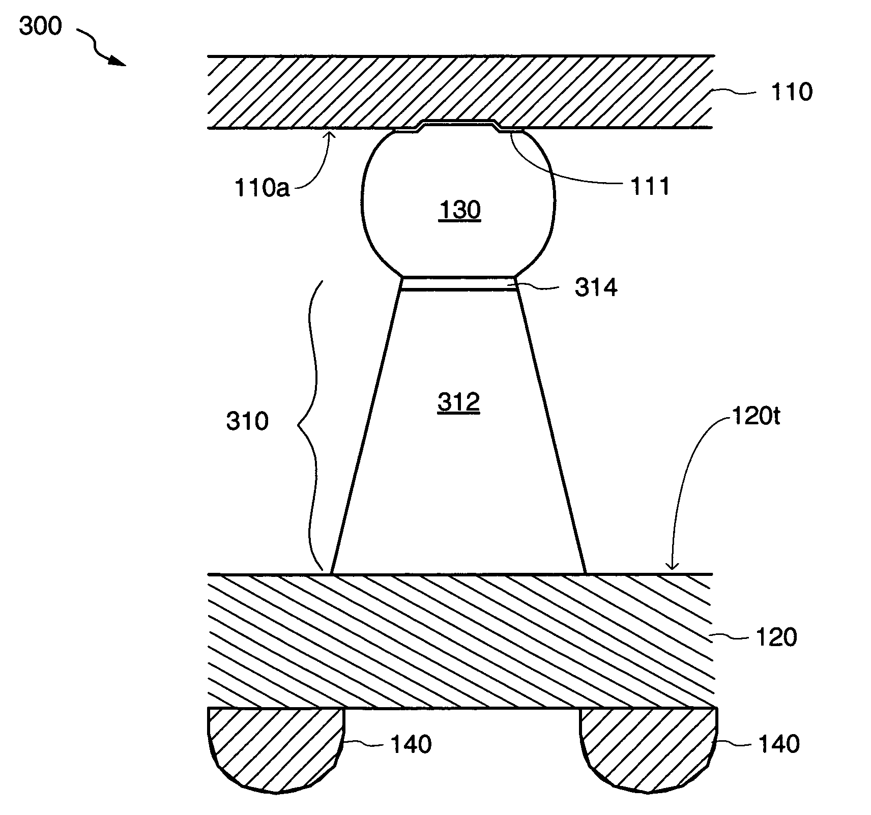
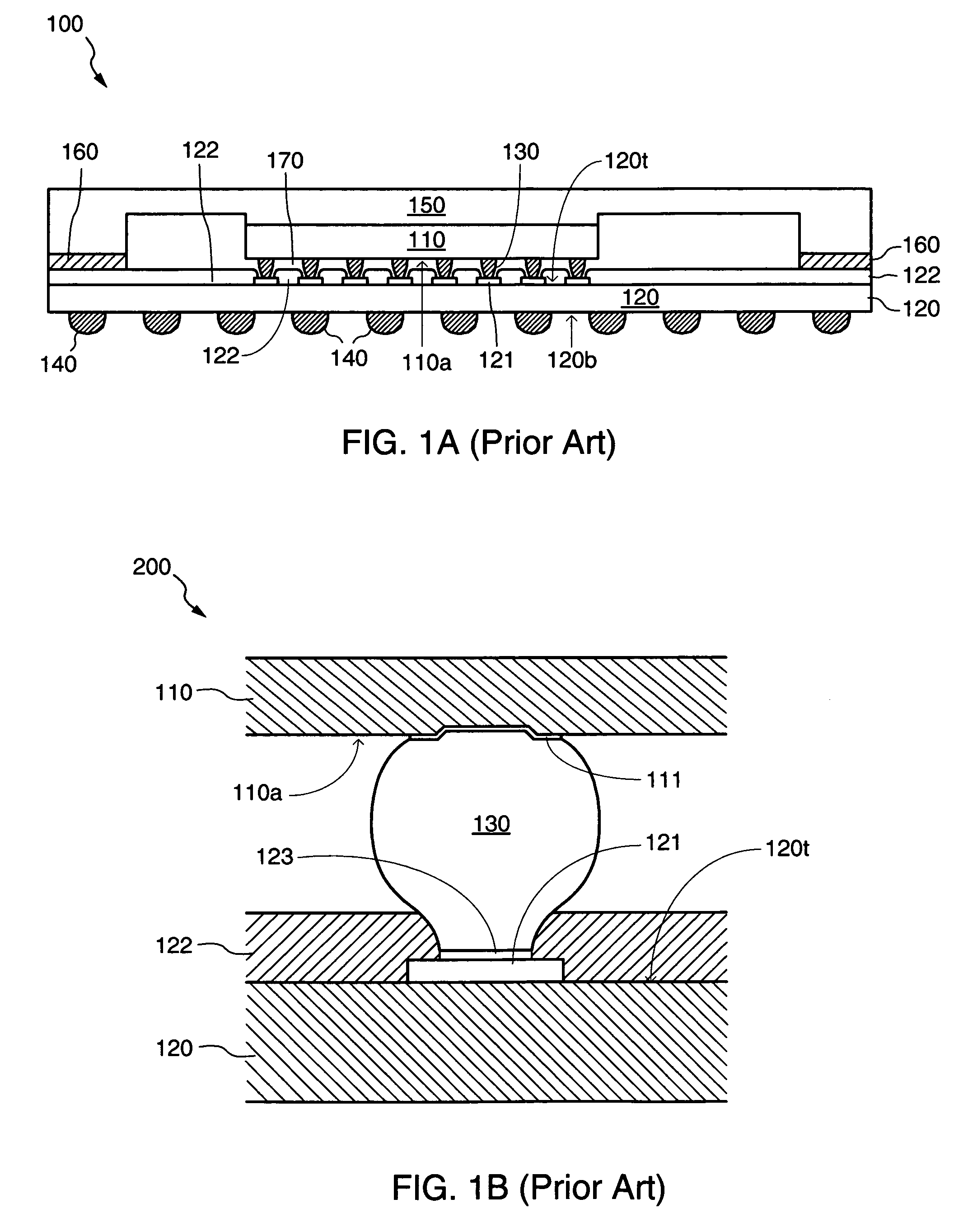
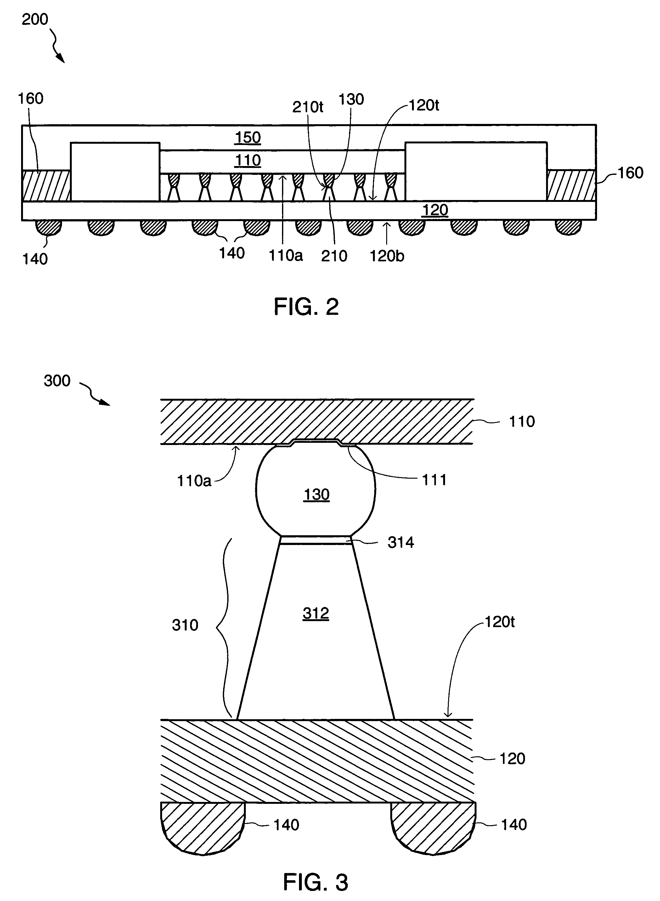
[0020]FIG. 2 shows a cross-sectional view of an IC package 200 having a die 110 flip-chip mounted to a substrate 120 in accordance with an embodiment of the present invention. Die 110, which may be formed using well-known techniques, may contain any suitable IC design such as, for example, a programmable l...


PUM


Abstract

A semiconductor package having a substrate and a die includes a plurality of conductive posts attached to the substrate and bonded to an active surface of the die via a plurality of corresponding microbumps. The conductive posts are flexible and extend beyond the top surface of the substrate a sufficient distance to absorb lateral forces exerted upon the microbumps.

Description

FIELD OF INVENTION[0001]The present invention relates generally to semiconductor devices, and more specifically to semiconductor packages containing integrated circuit dice.DESCRIPTION OF RELATED ART[0002]Typically, a plurality of integrated circuits (ICs) are formed on a semiconductor (e.g., silicon) wafer, which is then cut or “diced” to separate individual ICs from one another. The resulting bare IC dice (e.g., chips) are then packaged to protect them from external conditions. An IC package typically includes an IC die mounted on a substrate and encapsulated with a protective material. Conductive contacts formed on the die are electrically connected to corresponding pads formed on a first surface of the substrate. External leads formed on a second surface of the substrate and electrically connected to the pads on the first surface via the substrate's interconnect circuitry provide electrical connections to external systems (e.g., to other packaged dice) via a carrier such as a Pr...

Claims


Application Information

Patent Timeline
Patent Type & Authority Patents(United States)
IPC IPC(8): G01R31/02
CPCH01L21/563H01L23/10H01L23/3675H01L24/16H01L24/73H01L24/13H01L23/3128H01L24/32H01L24/81H01L2224/10175H01L2224/13016H01L2224/13147H01L2224/16225H01L2224/73204H01L2224/73253H01L2224/81193H01L2224/81385H01L2224/814H01L2224/81447H01L2224/81815H01L2924/01004H01L2924/01013H01L2924/01029H01L2924/01075H01L2924/01078H01L2924/01082H01L2924/14H01L2924/15311H01L2924/16152H01L2924/19041H01L2924/00014H01L2924/014H01L2224/131H01L2924/01033H01L2924/01014H01L2924/00H01L2924/3512H01L2224/16057H01L2224/0554H01L2224/05572H01L2224/05573H01L2224/05599H01L2224/0555H01L2224/0556
Inventor CONN, ROBERT O.CAREY, STEVEN J.
Owner XILINX INC
Why Eureka
Try Eureka