Integrated circuit with staggered differential wire bond pairs

a technology of differential wire bonding and integrated circuit, which is applied in the direction of electrical equipment, semiconductor devices, semiconductor/solid-state device details, etc., can solve the problems of limiting system data throughput, increasing substrate size and resulting package size, and substantial mutual coupling, etc., to achieve the effect of improving high-speed performance and techniques

Active Publication Date: 2010-03-09
BELL SEMICON LLC
View PDF8 Cites 6 Cited by
  • Summary
  • Abstract
  • Description
  • Claims
  • Application Information

AI Technical Summary

Benefits of technology

[0007]The present invention in an illustrative embodiment provides an integrated circuit having wire bonds that permit improved high speed performance and techniques for configuring such wire bonds in the integrated circuit.
[0010]Advantageously, an illustrative embodiment of the present invention produces wire bonds that allow for improved high speed performance. The wire bond configuration of the illustrative embodiment of the present invention decreases crosstalk by increasing the distance between data signal wire bond pairs. The distance is increased through the formation of alternating different wire bond profiles and staggered wedge bond spacings at the substrate for differential wire bond pairs. Due to the increased spatial separation, a wire-bond package has the ability to achieve data rates that otherwise would have required a flip-chip package. Further, less separation is required between wire bonds in a plan view, resulting in reduced size and cost for the die and substrate, and the packaged integrated circuit as a whole. Thus, the illustrative embodiment allows system performance needs to be met while providing a cost competitive integrated circuit package.

Problems solved by technology

Thus, wire bonds packed tightly together result in a substantial mutual coupling.
The noise generated by crosstalk in each interface may result in bit errors that limit the system data throughput.
However, this also increases substrate size and resulting package size, which is directly proportional to cost.

Method used


Image

  • Integrated circuit with staggered differential wire bond pairs
  • Integrated circuit with staggered differential wire bond pairs
  • Integrated circuit with staggered differential wire bond pairs

Examples


Embodiment Construction

[0021]As will be described in detail below, the present invention in the illustrative embodiment provides an integrated circuit having wire bonds configured for improved high speed performance, and techniques for forming such wire bonds in the integrated circuit. The phrase “differential pair,” as described herein, refers to two adjacent wire bonds having approximately the same wire bond profile reducing differential noise coupling and differential signal propagation delay. Further, the term “proximate,” as described herein, refers to neighboring or next in spacial order.

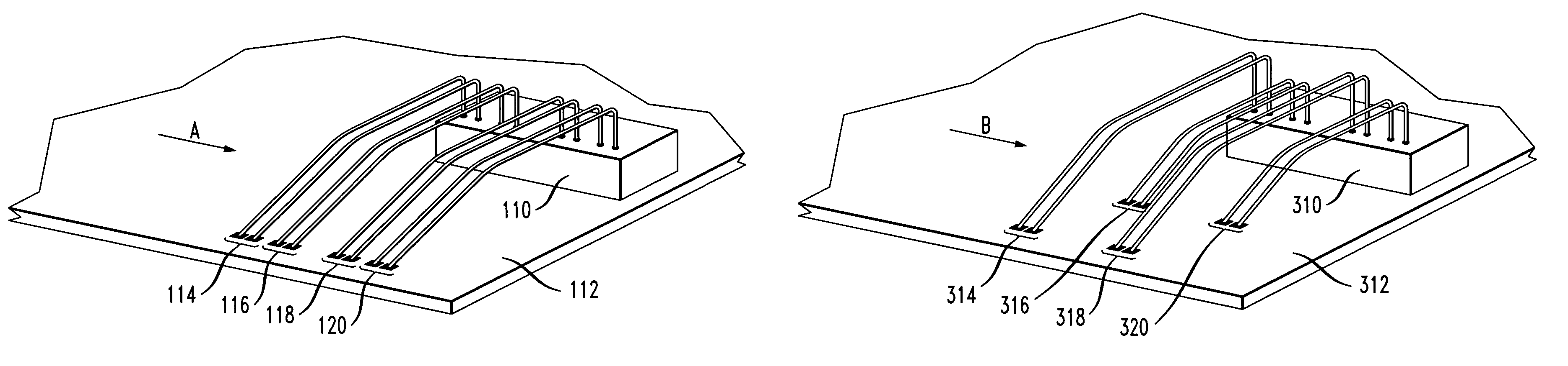
[0022]Referring initially to FIG. 1, a perspective view of an integrated circuit having long arc differential wire bond pairs is illustrated. A die 110 is disposed in a packaged integrated circuit on a substrate 112. Much of the integrated circuit packaging is not shown so that the internal elements and wires are visible.

[0023]In many applications, it is desirable to ensure a high immunity to noise, since parasitic ...


PUM


Abstract

An integrated circuit comprises an integrated circuit package and one or more circuit elements disposed within the integrated circuit package. The integrated circuit also comprises at least two differential wire bond pairs providing connections for at least one of the one or more circuit elements. Proximate differential wire bond pairs of the at least two differential wire bond pairs have substantially different wire bond profiles.

Description

FIELD OF THE INVENTION[0001]The present invention relates generally to the field of integrated circuits and, more particularly, to wire-bonding operations performed on an integrated circuit.BACKGROUND OF THE INVENTION[0002]An integrated circuit may include multiple transistor die that are placed in an integrated circuit package by a die attach machine. A robotic bonding tool may be used to wire bond the die to a package substrate, leads of a package leadframe, or other circuit elements within the package. Such a tool generally includes a surface / wire-feed detection system that detects bond pads or other bond sites of a given die. The other circuit elements in an integrated circuit may include, for example, tuning capacitors.[0003]The wire bonding of the various circuit elements may create several differently-shaped wire bond profiles, depending on the placement of the various circuit elements to be connected by wire bonds. A wire bond profile may be characterized as a side or profil...

Claims


Application Information

Patent Timeline
Patent Type & Authority Patents(United States)
IPC IPC(8): H01L23/495
CPCH01L23/66H01L24/49H01L24/85H01L2223/6611H01L2224/4809H01L2224/48095H01L2224/48227H01L2224/48465H01L2224/49175H01L2224/49433H01L2224/85H01L2924/01005H01L2924/19041H01L2924/30105H01L2924/30107H01L2924/00014H01L24/48H01L2924/01033H01L2224/78H01L2924/00012H01L2924/00H01L2224/49052H01L2224/49176H01L2924/14H01L2224/45099H01L2224/05599
Inventor APPEL, GAVINREBELO, ASHLEYWITTENSOLDNER, CHRISTOPHER J.
Owner BELL SEMICON LLC
Why Eureka
Try Eureka