
Photoactive compounds

a technology of photoactive compounds and compounds, applied in the field of photoactive compounds, can solve the problems of critical roughness of photoresist patterns, adverse effects of edge roughness on the lithographic performance of photoresist,

Inactive Publication Date: 2010-03-16
MERCK PATENT GMBH
View PDF45 Cites 58 Cited by
  • Summary
  • Abstract
  • Description
  • Claims
  • Application Information

AI Technical Summary

Benefits of technology

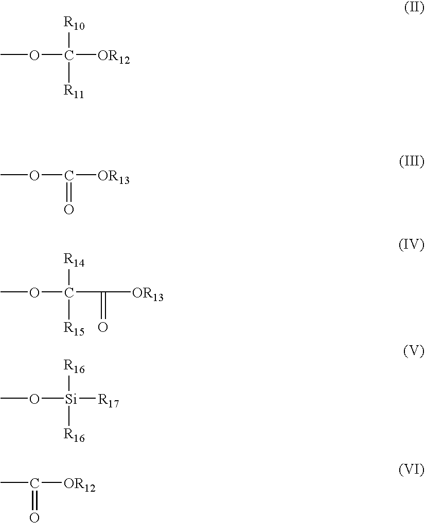
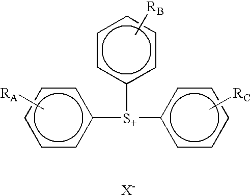
The present invention is about a new compound that can be used in a photoresist composition for imaging in deep UV. The compound has a specific formula and can be used with a polymer that contains an acid labile group. The photoresist composition can be used to image a substrate by coating it with the compound and then exposing it to light. The compound helps to improve the resolution and accuracy of the image. The invention also includes a process for using the photoresist composition to image a substrate.

Problems solved by technology

Thus, treatment of an exposed negative-working resist with a developer causes removal of the non-exposed areas of the photoresist coating and the creation of a negative image in the coating, thereby uncovering a desired portion of the underlying substrate surface on which the photoresist composition was deposited.
In cases where the photoresist dimensions have been reduced to below 150 nm, the roughness of the photoresist patterns has become a critical issue.
Edge roughness can have adverse effects on the lithographic performance of the photoresist, especially in reducing the critical dimension latitude and also in transferring the line edge roughness of the photoresist to the substrate.

Method used


Image

  • Photoactive compounds
  • Photoactive compounds
  • Photoactive compounds

Examples


example 1

Synthesis of bis[4-acetyloxyphenyl]phenylsulfonium perfluorobutanesulfonate

[0076]Bis[4-hydroxylphenyl]phenysulfonium perfluorobutanesulfonate (10 g) and acetone were placed into a reaction vessel equipped with an agitator, a thermometer, a reflux condenser, and a tube for introducing nitrogen gas into the vessel. Under a nitrogen blanket, 4.6 g of potassium carbonate was added to the reaction vessel and the mixture was stirred for an hour. Acetic anhydride 3.43 gram was added and stirred overnight at room temperature. Dichloromethane (150 ml) and water were added to the reaction vessel and the mixture was stirred for 2 hours. The mixture was then placed into a separatory funnel and the organic (dichloromethane) layer was retained. The dichloromethane layer was washed several times with water, dried over anhydrous sodium sulfate, filtered, and the remaining volatile materials were evaporated to leave an oil. Ether was added to the oil and the mixture was stirred vigorously. A very st...

example 2

Synthesis of bis[4-acetyloxyphenyl]phenylsulfonium 4-(1,1,1,2-tetrafluoroethoxy)perfluorobutanesulfonate

[0078]This material was made following Example 1 except bis[4-hydroxyphenyl]phenysulfonium 4-(1,1,1,2-tetrafluoroethoxy)perfluorobutanesulfonate was used instead of bishydroxylphenylphenysulfonium perfluorobutanesulfonate

[0079]

[0080]In addition, the following compounds can be made following the procedure in Example 2 using the corresponding anion:

[0081][0082]Example 2a: Where X═CF3SO3[0083]Example 2b: Where X═N(SO2CF3)2 [0084]Example 2c: Where X=N(SO2C2F5)2 [0085]Example 2d: Where X═N(SO2CF3)(SO2C4F9)[0086]Example 2e: Where X═N(SO2C3F7)2 [0087]Example 2f: Where X═C(SO2CF3)3 [0088]Example 2g: Where X═CH3CH3CH3O(CF2)4SO3 [0089]Example 2h: Where X═C4F9SO3

example 3

Synthesis of bis[2-methyladamantylacetyloxymethoxyphenyl]phenylsulfonium perfluorobutanesulfonate

[0090]This material was made following the procedure in Example 1 except 2-methyladamantylbromoacetate was used in place of acetic anhydride.

[0091]

[0092]In addition, the following compounds can be made following the procedure in Example 3 using the corresponding anion:

[0093][0094]Example 3a: Where X═CF3CHFO(CF2)4SO3 [0095]Example 3b: Where X═CF3SO3 [0096]Example 3c: Where X═N(SO2CF3)2 [0097]Example 3d: Where X═N(SO2C2F5)2 [0098]Example 3e: Where X═N(SO2CF3)(SO2C4F9)[0099]Example 3f: Where X═N(SO2C3F7)2 [0100]Example 3g: Where X═CH3CH3CH3O(CF2)4SO3 [0101]Example 3h: Where X═C(SO2CF3)3 [0102]Example 3i: Where X═C4F9SO3


PUM

PropertyMeasurementUnit
exposure wavelengthaaaaaaaaaa
roughnessaaaaaaaaaa
wavelengthsaaaaaaaaaa

Abstract

The present invention relates to novel photoacid generators.

Description

CROSS-REFERENCE TO RELATED APPLICATION[0001]This application is a continuation-in-part application of Ser. No. 11 / 280,842, filed Nov. 16, 2005, now abandoned the contents of which are hereby incorporated herein by reference.FIELD OF INVENTION[0002]The present invention relates to novel photoactive compounds useful in photoresist compositions in the field of microlithography, and especially useful for imaging negative and positive patterns in the production of semiconductor devices, as well as photoresist compositions and processes for imaging photoresists.BACKGROUND OF THE INVENTION[0003]Photoresist compositions are used in microlithography processes for making miniaturized electronic components such as in the fabrication of computer chips and integrated circuits. Generally, in these processes, a thin coating of film of a photoresist composition is first applied to a substrate material, such as silicon wafers used for making integrated circuits. The coated substrate is then baked to...

Claims


Application Information

Patent Timeline
Patent Type & Authority Patents(United States)
IPC IPC(8): G03F7/004C07C381/12
CPCC07C309/06C07C309/10C07C311/48C07C317/04C07C381/12G03F7/0045G03F7/0392G03F7/0395C08K5/375C07C2103/74Y10S430/115Y10S430/122Y10S430/126Y10S430/114C07C2603/74G03F7/0046
Inventor RAHMAN, M. DALILPADMANABAN, MUNIRATHNA
Owner MERCK PATENT GMBH
Learn More