Integrated optical device and fabrication method thereof

a technology of integrated optical devices and fabrication methods, which is applied in the direction of lasers, semiconductor lasers, semiconductor/solid-state device testing/measurement, etc., can solve the problems of reduced optical coupling efficiency of semiconductor lasers and optical modulators, difficult to match the height position of the absorption layer of the optical modulator with the height position of the active layer of the semiconductor laser, and difficult to control the etching depth, etc., to achieve the effect of improving the optical coupling efficiency between the firs

Inactive Publication Date: 2010-03-16
SUMITOMO ELECTRIC IND LTD
View PDF5 Cites 2 Cited by
  • Summary
  • Abstract
  • Description
  • Claims
  • Application Information

AI Technical Summary

Benefits of technology

[0009]In addition, in the step of forming the first semiconductor optical element, Al element is preferably detected by using the plasma emission spectra. As a result, Al element can be detected without affecting the plasma state when performing the dry etching.
[0013]If a side etch is formed, it is possible to suppress the anomalous growth in an upward direction of crystals which are contained in the second semiconductor optical element along the side wall of the first semiconductor optical element when forming the second semiconductor optical element. As a result, because the second semiconductor optical element is suitably optically coupled to the first semiconductor optical element, the coupling efficiency improves.
[0019]In the case of the integrated optical device of the present invention, because the height position of the second semiconductor optical element is easily matched with the height position of the first semiconductor optical element during fabrication, the optical coupling efficiency between the first semiconductor optical element and second semiconductor optical element can be improved.

Problems solved by technology

However, the above method makes it difficult to control the etching depth when dry-etching the n-type cladding layer, active layer, and p-type cladding layer.
In addition, when the fluctuations in the etching depth are large, it is difficult to match the height position of the absorption layer of the optical modulator with the height position of the active layer of the semiconductor laser.
As a result, the optical coupling efficiency of the semiconductor laser and optical modulator is reduced.

Method used


Image

  • Integrated optical device and fabrication method thereof
  • Integrated optical device and fabrication method thereof
  • Integrated optical device and fabrication method thereof

Examples


first embodiment

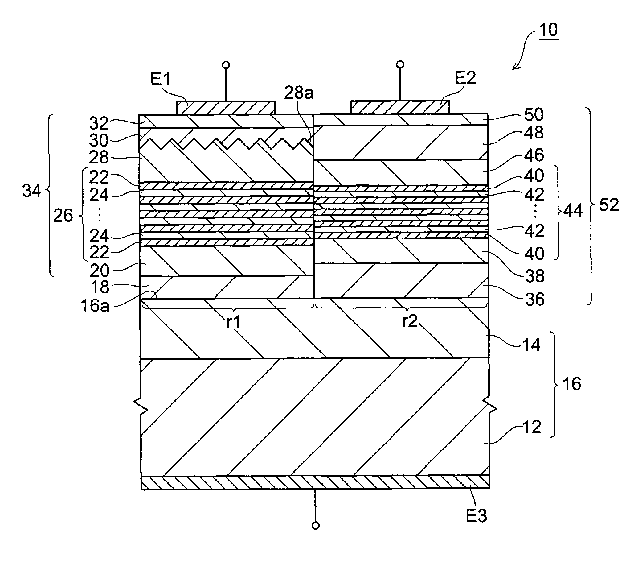
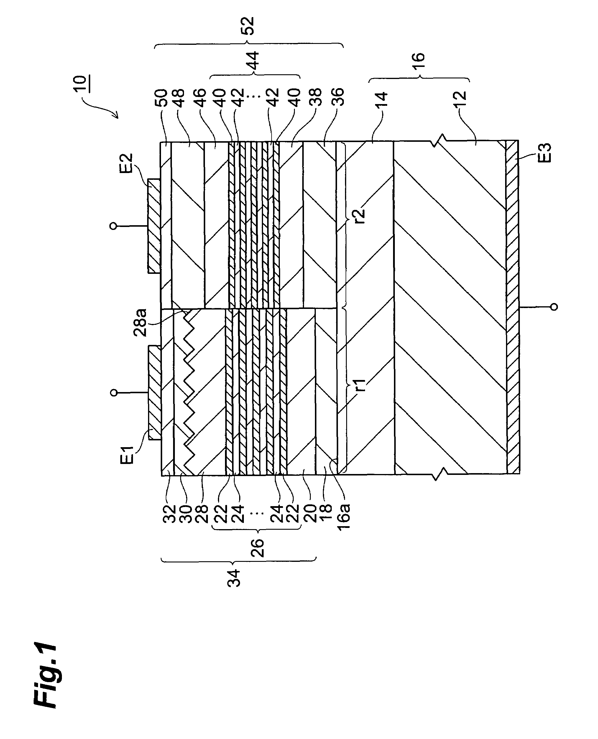
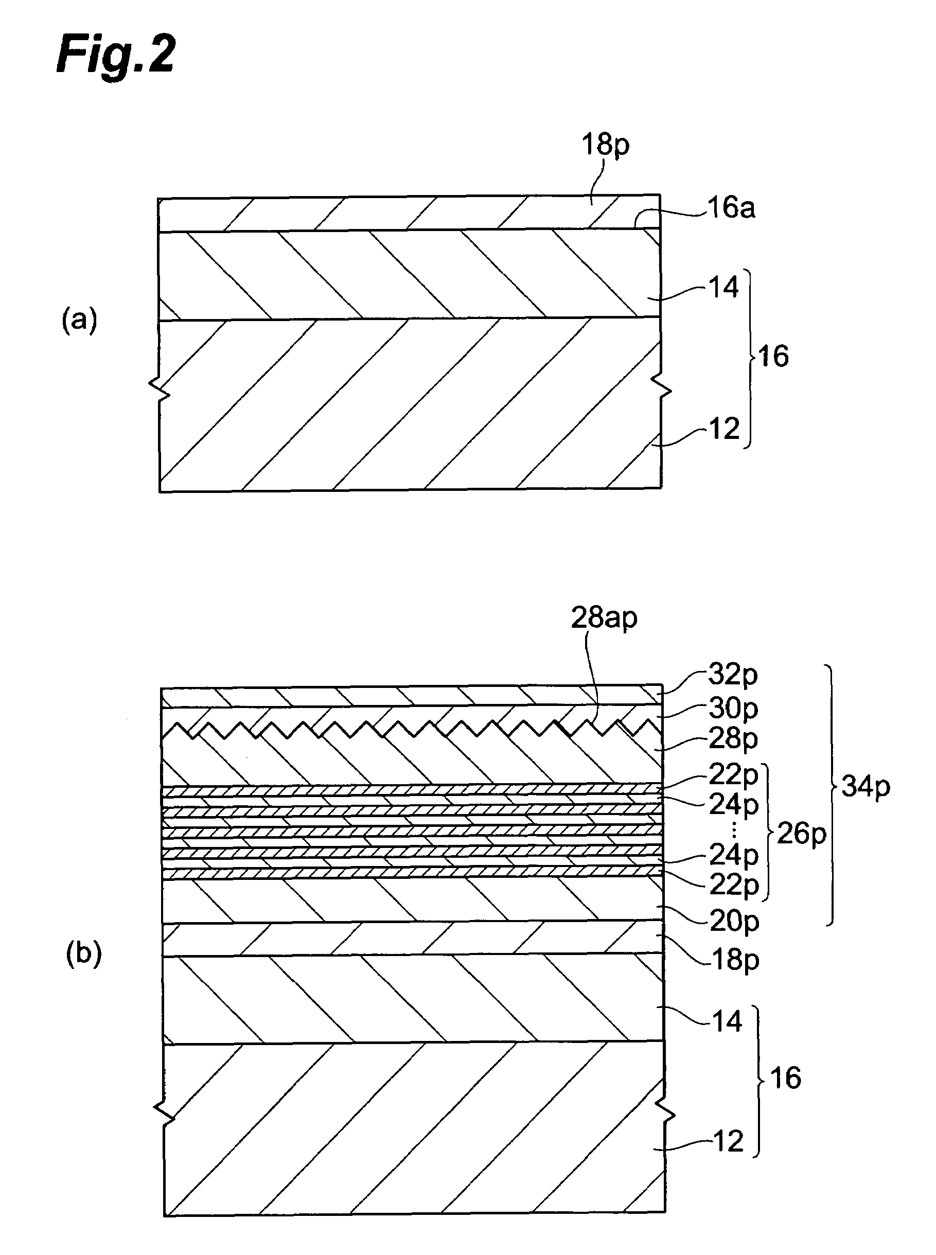
[0031]FIG. 1 is a cross-sectional view that schematically shows an example of an integrated optical device according to the The integrated optical device 10 shown in FIG. 1 comprises a first semiconductor optical element 34 that is provided on a first region r1 of a main face 16a of a substrate 16 and a second semiconductor optical element 52 that is provided on a second region r2 of the main face 16a of substrate 16. The semiconductor optical element 52 is optically coupled to semiconductor optical element 34. Therefore, the integrated optical device 10 has a butt joint structure. Further, a III-V compound semiconductor layer 18 including Al element is provided between substrate 16 and the semiconductor optical element 34. Electrodes E1 and E2 are each provided on the semiconductor optical element 34 and semiconductor optical element 52. An electrode E3 is provided on the underside of the substrate 16.

[0032]Substrate 16 comprises a substrate main body 12 and a buffer layer 14 whic...

second embodiment

[0058]FIG. 5 is a cross-sectional view that schematically shows an example of an integrated optical device according to the The integrated optical device 110 shown in FIG. 5 comprises a first semiconductor optical element 134 that is provided on a first region r1 of main face 16a of the substrate 16 and a second semiconductor optical element 152 that is provided on a second region r2 of main face 16a of substrate 16. The semiconductor optical element 152 is optically coupled to the semiconductor optical element 134. Therefore, the integrated optical device 110 has a butt joint structure. Further, a III-V compound semiconductor layer 118 containing Al element is provided between the substrate 16 and semiconductor optical element 134. Electrodes E1 and E2 are each provided on the semiconductor optical element 134 and semiconductor optical element 152. Electrode E3 is provided on the underside of the substrate 16.

[0059]The semiconductor optical element 134 comprises an optical confine...


PUM


Abstract

An integrated optical device comprising a first semiconductor optical element provided on a first region of the main face of a substrate and a second semiconductor optical element provided on a second region and optically coupled to the first semiconductor optical element is fabricated. A first III-V compound semiconductor layer containing Al element is formed on the main face. A second III-V compound semiconductor layer for forming the first semiconductor optical element is then formed on the first III-V compound semiconductor layer. An etching mask M is formed on the first region. The end point of the dry etching is detected by using the etching mask M to dry-etch the second III-V compound semiconductor layer while detecting Al element. The first semiconductor optical element is thus formed. The second semiconductor optical element is formed on the second region.

Description

BACKGROUND OF THE INVENTION[0001]1. Field of the Invention[0002]The present invention relates to an integrated optical device and a fabrication method thereof.[0003]2. Related Background Art[0004]Integrated optical devices that have a semiconductor laser and an optical modulator that is optically coupled to the semiconductor laser provided on a substrate are known (See Japanese Application Laid Open No. H7-263655). Structures for implementing this optical coupling include Butt joint structures. This type of structure is formed as follows. First, an n-type cladding layer, an active layer and p-type cladding layer are formed on a substrate. Thereafter, an etching mask is formed on a p-type cladding layer in a region for forming a semiconductor laser. The n-type cladding layer, active layer and p-type cladding layer in a region for forming an optical modulator are then removed by means of dry etching by using the etching mask. Thereafter, an n-type cladding layer, absorption layer, and...

Claims


Application Information

Patent Timeline
Patent Type & Authority Patents(United States)
IPC IPC(8): H01L21/00H01S5/12
CPCB82Y20/00H01L22/26H01L27/15H01S5/0265H01S5/12H01S5/34306
Inventor KATSUYAMA, TOMOKAZU
Owner SUMITOMO ELECTRIC IND LTD
Why Eureka
Try Eureka