Pendeo epitaxial structures and devices

a technology of epitaxial structure and device, applied in the direction of basic electric elements, semiconductor devices, electrical apparatus, etc., can solve the problems of reducing the scope of process conditions that are available for lateral growth, and limiting the available temperatur

Active Publication Date: 2010-03-23
CREE INC
View PDF16 Cites 36 Cited by
  • Summary
  • Abstract
  • Description
  • Claims
  • Application Information

AI Technical Summary

Benefits of technology

[0042]a growth-blocking layer on said convex shoulders, whereby said growth-blocking layer suppresses vertical and angular growth from said convex shoulders, to accommodate lateral epitaxial overgrowth across the trench cavity above said convex shoulders.

Problems solved by technology

Unfortunately, when Pendeo epitaxial techniques are applied to gallium nitride (GaN) on heteroepitaxial substrates, the etching of the trench must extend downwardly into the heteroepitaxial substrate and the growth temperature must be very high in order to reduce parasitic growth in the center of the trench.
Increasing the required etching time, particularly when the substrate is a sapphire substrate or a substrate of similar material, and limiting the available temperature to accommodate such substrate, as required for the use of Pendeo epitaxial techniques, poses problems.
Even if a GaN homoepitaxial substrate is employed for the Pendeo epitaxial growth process, these problems remain.
If the etched trench is not sufficiently deep, parasitic growth can damage the lateral layer and the range of process conditions that are available for lateral growth is greatly reduced in scope, so that vertical growth in the window region cannot occur.

Method used


Image

  • Pendeo epitaxial structures and devices
  • Pendeo epitaxial structures and devices
  • Pendeo epitaxial structures and devices

Examples


example 1

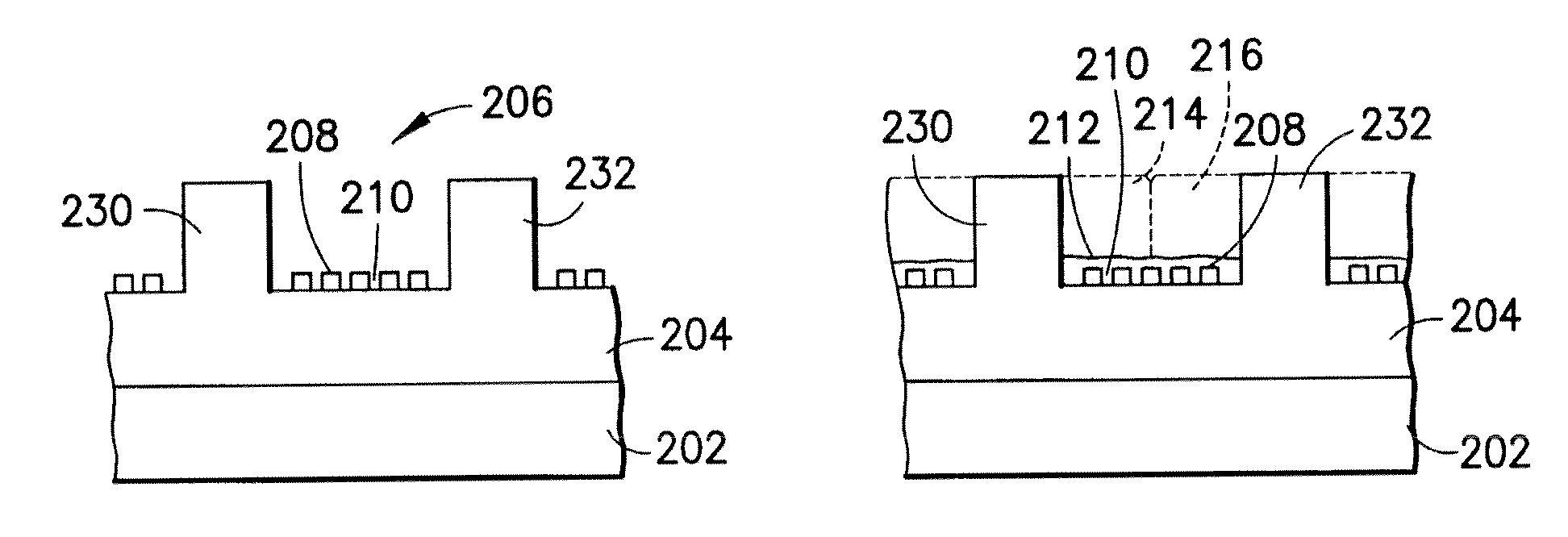
Pendeo Epitaxy with 15 Micron Wide Reduced Defect Density Stripes Formed on GaN Substrate

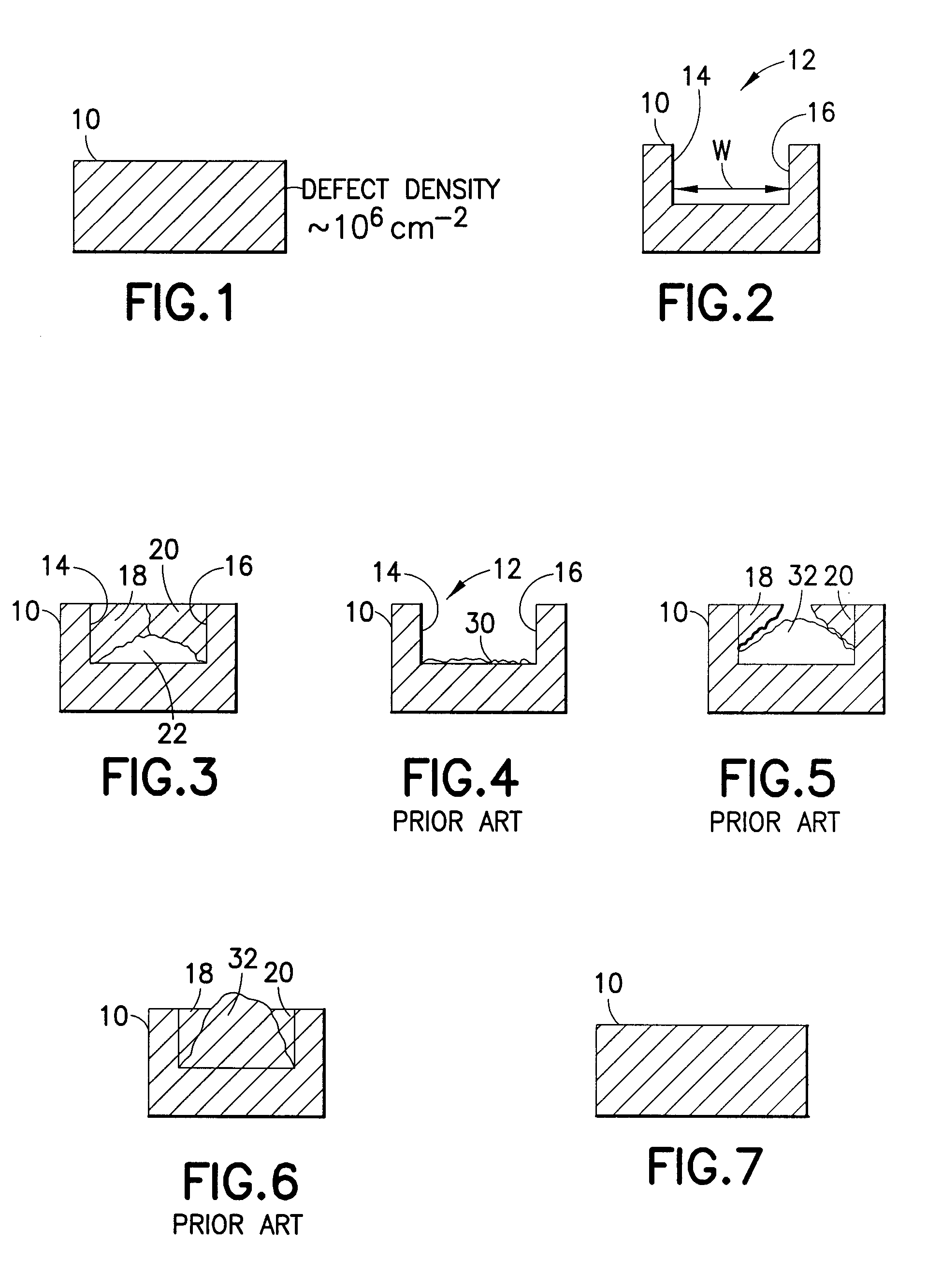
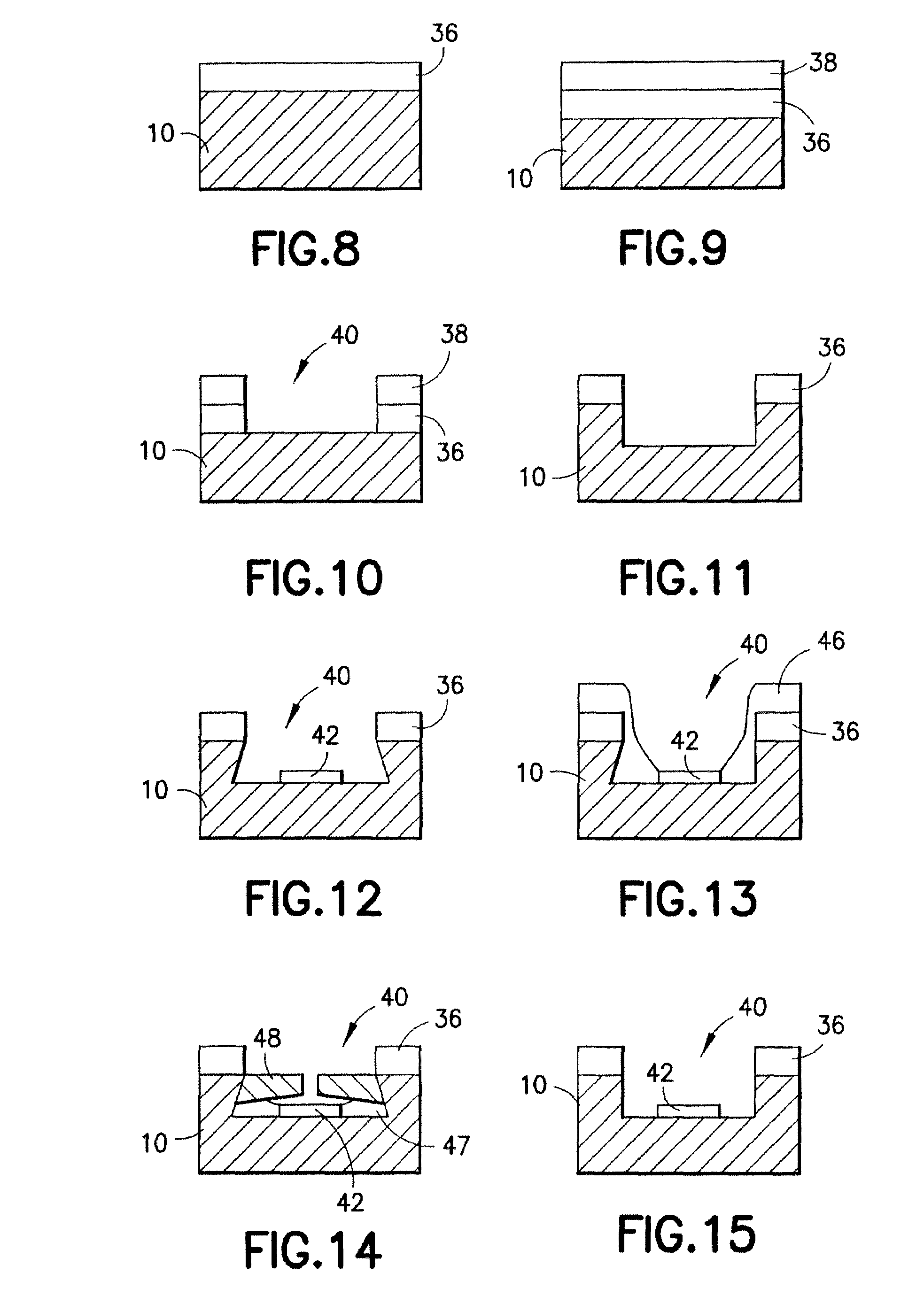
[0106]A free-standing, two-inch diameter GaN substrate with reduced dislocation density in the striped region may be made using the following illustrative process. To safely obtain the best results, a proper processing environment such as found in a semiconductor clean room, as well as proper gear for handling and storing the wafer, and proper protective gear, are employed.

[0107]A two-inch diameter HVPE GaN substrate (wafer) is obtained and cleaned using an RCA clean. The RCA clean is a standard clean in the semiconductor industry and consists of an organic clean performed with a 5:1:1 H2O: H2O2: NH4OH solution at 80 C, an oxide strip performed with a 50:1 H2O: HF solution at room temperature and an ionic clean performed with a 6:1:1 H2O: H2O2: HCl solution at 80° C. Photoresist is deposited on the cleaned wafer using standard techniques. The wafer is patterned using a contact aligner and a mask...


PUM


Abstract

A substrate comprising a trench lateral epitaxial overgrowth structure including a trench cavity, wherein the trench cavity includes a growth-blocking layer or patterned material supportive of a coalescent Pendeo layer thereon, on at least a portion of an inside surface of the trench. Such substrate is suitable for carrying out lateral epitaxial overgrowth to form a bridged lateral overgrowth formation overlying the trench cavity. The bridged lateral overgrowth formation provides a substrate surface on which epitaxial layers can be grown in the fabrication of microelectronic devices such as laser diodes, high electron mobility transistors, ultraviolet light emitting diodes, and other devices in which low dislocation density is critical. The epitaxial substrate structures of the invention can be formed without the necessity for deep trenches, such as are required in conventional Pendeo epitaxial overgrowth structures.

Description

FIELD OF THE INVENTION[0001]The present invention relates to Pendeo epitaxial growth and to microelectronic devices including Pendeo epitaxial films, such as laser diodes, high electron mobility transistors (HEMTs), ultraviolet light emitting diodes, and other devices in which low dislocation density is critical.DESCRIPTION OF THE RELATED ART[0002]Lateral epitaxy overgrowth (LEO) is a known technique to reduce dislocations in epitaxial thin films, leading to improved performance and reliability. Pendeo epitaxy is a specialized form of lateral epitaxy overgrowth. Traditional lateral epitaxial overgrowth techniques require a period of vertical growth followed by horizontal growth. Pendeo growth utilizes an etched trench, thereby eliminating the need for an initial vertical growth step. The resulting simplification in the growth cycle produces fewer defective films, shorter growth periods and better uniformity of the product films.[0003]Trench lateral epitaxial overgrowth (LEO) is a pr...

Claims


Application Information

Patent Timeline
Patent Type & Authority Patents(United States)
IPC IPC(8): H01L21/20
CPCH01L21/0237H01L21/0254H01L21/02639H01L21/0265H01L29/66462H01L29/2003
Inventor BRANDES, GEORGE R.CHAKRABORTY, ARPANNAKAMURA, SHUJIHANSEN, MONICADENBAARS, STEVEN
Owner CREE INC
Why Eureka
Try Eureka