Nonvolatile semiconductor memory device
a semiconductor and memory device technology, applied in semiconductor devices, digital storage, instruments, etc., can solve the problems of insufficient low voltage for programming or erasing action, resistance value decrease, resistance value decrease, etc., and achieve the effect of shortening the application tim
- Summary
- Abstract
- Description
- Claims
- Application Information
AI Technical Summary
Benefits of technology
Problems solved by technology
Method used
Image


Examples
first embodiment
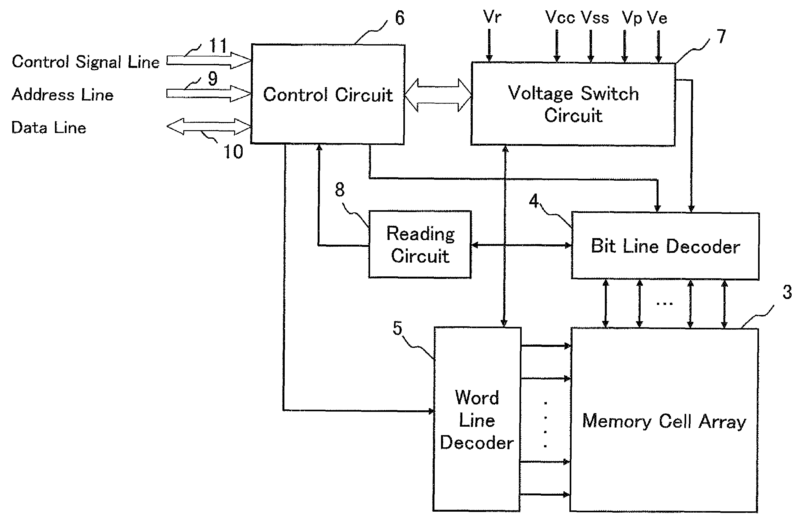
[0146]FIG. 10 schematically shows one constitution example of the device of the present invention. In addition, in FIG. 10, the same references are allotted to the components common to those of the conventional nonvolatile semiconductor memory device in the following description. As shown in FIG. 10, the device comprises a bit line decoder 4, a word line decoder 5, a voltage switch circuit 7a, a reading circuit 8, and a control circuit 6a in the periphery of a cross-point type memory cell array 3 in which 1R type memory cells (not shown) are arranged in the form of a matrix. Basically, it has the same constitution as that of the conventional nonvolatile semiconductor memory device provided with the memory cell array comprising 1R type memory cells shown in FIG. 2. It is different from the conventional nonvolatile semiconductor memory device shown in FIG. 2 in a voltage applied from the voltage switch circuit 7a to the memory cell array 3, its timing action, and the operation of the ...
example 1
[0155]In an Example 1, a description will be made of a process in a case where the application of the programming voltage Vp to the selected memory cell M0 (programming period Tp), the application of the programming compensating voltage Vpc to the first unselected memory cells M1 (first programming compensating period Tpc1), the application of the programming compensating voltage Vpc to the second unselected memory cells M2 (second programming compensating period Tpc2) are performed in a time-division manner, at the time of programming action in one selected period until the selection of the selected memory cell is switched to another selected memory cell, with reference to FIG. 12. In addition, it is to be noted that in the example that the first programming compensating period Tpc1 and the second programming compensating period Tpc2 are the same or almost the same length as the programming period Tp. That is, Tp=Tpc1=Tpc2 or Tp≅Tpc1≅Tpc2.
[0156]FIG. 12 shows voltage changes of a vo...
example 2
[0166]In an Example 2, a description will be made of another process in a case where the application of the programming voltage Vp to the selected memory cell M0 (programming period Tp), the application of the programming compensating voltage Vpc to the first unselected memory cells M1 (first programming compensating period Tpc1), the application of the programming compensating voltage Vpc to the second unselected memory cells M2 (second programming compensating period Tpc2) are performed in a time-division manner, at the time of programming action in one selected period until the selection of the selected memory cell is switched to another selected memory cell, with reference to FIG. 13. In addition, it is to be noted that in the example 2 that the first programming compensating period Tpc1 and the second programming compensating period Tpc2 are the same or almost the same length as the programming period Tp. That is, Tp=Tpc1=Tpc2 or Tp≅Tpc1≅Tpc2.
[0167]FIG. 13 shows voltage changes...
PUM
 Abstract
Description
Claims
Application Information
 - R&D
- Intellectual Property
- Life Sciences
- Materials
- Tech Scout
- Unparalleled Data Quality
- Higher Quality Content
- 60% Fewer Hallucinations
Browse by: Latest US Patents, China's latest patents, Technical Efficacy Thesaurus, Application Domain, Technology Topic, Popular Technical Reports.
© 2025 PatSnap. All rights reserved.Legal|Privacy policy|Modern Slavery Act Transparency Statement|Sitemap|About US| Contact US: help@patsnap.com