Nitride semiconductor light emitting device and manufacturing method thereof

a light emitting device and semiconductor technology, applied in semiconductor lasers, solid-state devices, lasers, etc., can solve the problems of complex manufacturing process, high cost, and insufficient effect of improving light emission output, etc., to achieve low forward voltage (vf) and high light emission output

Active Publication Date: 2010-04-20
SHARP FUKUYAMA LASER CO LTD
View PDF28 Cites 3 Cited by
  • Summary
  • Abstract
  • Description
  • Claims
  • Application Information

AI Technical Summary

Benefits of technology

[0013]According to the present invention, a nitride semiconductor light emitting device having low forward voltage (Vf) and exhibiting high light emission output can be obtained.

Problems solved by technology

Therefore, the layer tends to contain much dislocation and defects.
When the n-side first multi-layered film layer is stacked in contact with the n-type contact layer, it would undesirably be influenced by the dislocation or defects, and sufficient effect of improving light emission output would not be attained.
When two different types of multi-layered films are grown, manufacturing process becomes complicated and the manufacturing cost increases.
In addition, stacking of a nitride semiconductor layer containing In on the n-side of the active layer induces dislocation and defects of In, which affects crystallinity of the active layer and possibly causes decrease in light emission output.

Method used


Image

  • Nitride semiconductor light emitting device and manufacturing method thereof
  • Nitride semiconductor light emitting device and manufacturing method thereof
  • Nitride semiconductor light emitting device and manufacturing method thereof

Examples


example 1

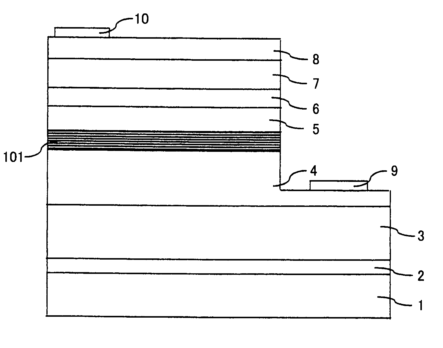
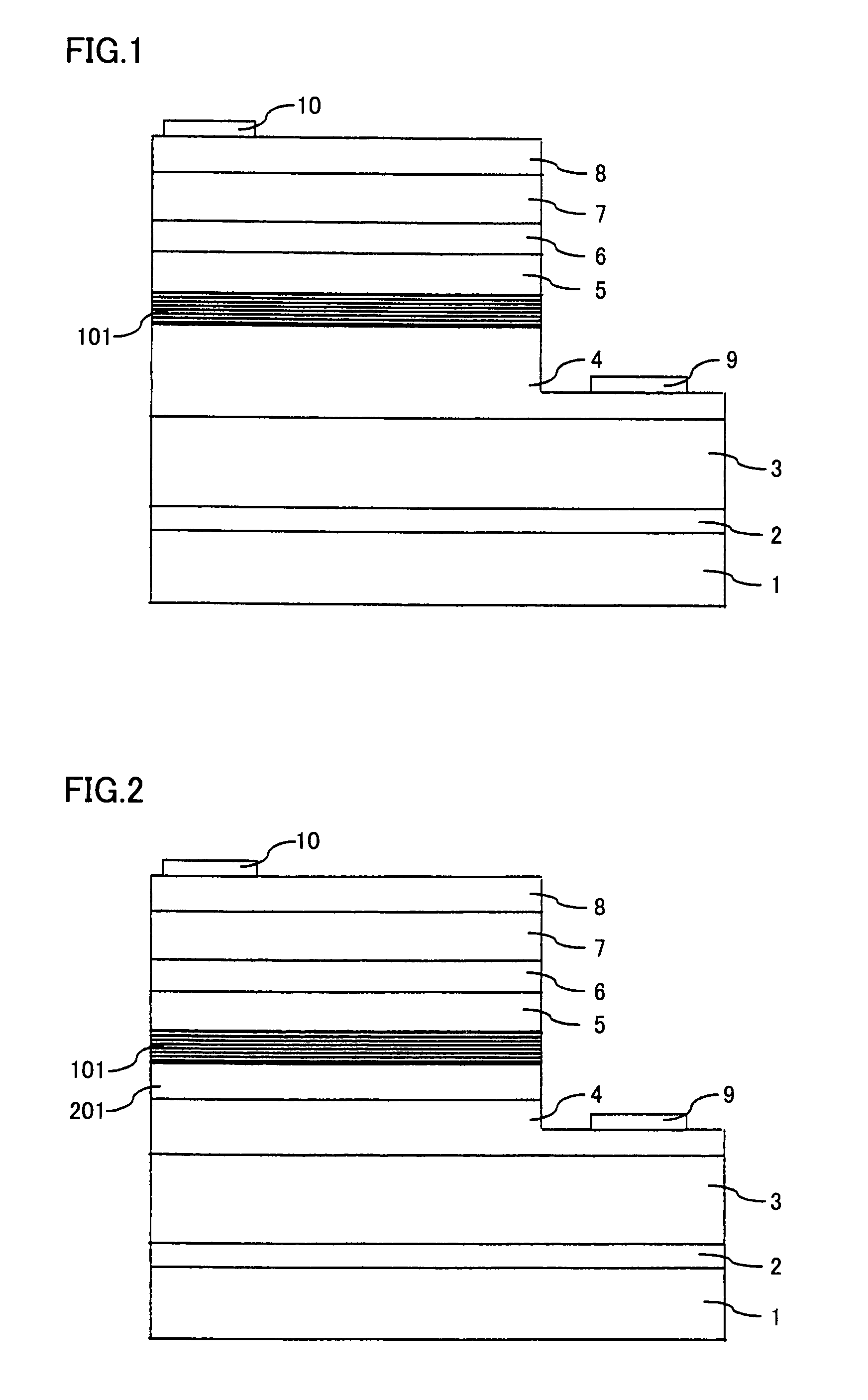
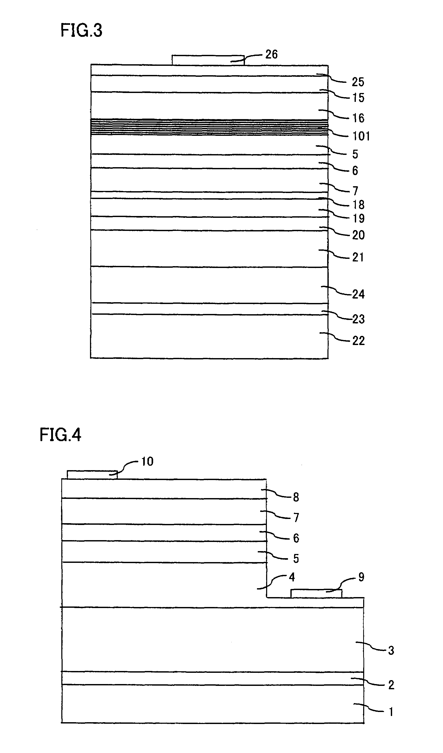
[0070]In the present example, a nitride semiconductor light emitting device having the structure shown in FIG. 2 was formed.

[0071](Buffer Layer 2)

[0072]First, a substrate 1 of sapphire (C plane) was set in a reaction furnace of an MOCVD apparatus, hydrogen was caused to flow while the growth temperature was increased to 1050° C., so that the substrate was cleaned. Next, the growth temperature was decreased to 510° C., and using hydrogen as the carrier gas and ammonia and TMG (trimethyl gallium) as the raw material gases, a buffer layer 2 of GaN was grown to the thickness of about 200 A, on substrate 1.

[0073](Underlying n-Type GaN Layer 3)

[0074]Then, the growth temperature was increased to 1050° C., and using hydrogen as the carrier gas, ammonia and TMG as the raw material gases and silane as the impurity gas, underlying n-type GaN layer 3 of GaN doped with Si to a concentration of 1×10¹⁸ / cm3 was grown to the thickness of 6 μm.

[0075](N-Type Contact Layer 4)

[0076]Next, under the same ...

example 2

[0102]In the present example, a nitride semiconductor light emitting device having the structure shown in FIG. 1 was formed. Specifically, an LED as the nitride semiconductor light emitting device of the present invention was formed through the same method as Example 1 except that n-type nitride semiconductor layer 201 of FIG. 2 was not formed.

[0103]The resulting LED exhibited emission wavelength of 460 nm, emission output of 4.7 mW and forward voltage Vf of 4.0V, when operated with forward current of 20 mA. Though light emission output was lower than that of Example 1, the light emission output was improved than Comparative Example 1, and it can be seen that the effect of improving light emission output of the present invention was sufficiently attained.

example 3

[0104]In the present example, a nitride semiconductor light emitting device having the structure shown in FIG. 2 was formed. Specifically, an LED as the nitride semiconductor light emitting device of the present invention was formed through the same method as Example 1 except that a GaN layer having the thickness of 20 nm and doped with Si to a concentration of 1×10¹⁸ / cm3 was formed in place of the undoped GaN layer, as the second nitride semiconductor layer of multi-layered nitride semiconductor layer 101.

[0105]The resulting LED exhibited emission wavelength of 460 nm, emission output of 5 mW and forward voltage Vf of 4.0V, when operated with forward current of 20 mA, that is, the same properties as attained by Example 1.


PUM

PropertyMeasurementUnit
temperatureaaaaaaaaaa
thicknessaaaaaaaaaa
thicknessaaaaaaaaaa

Abstract

An object is to provide a nitride semiconductor light emitting device capable of attaining high light emission output while lowering Vf, as well as to provide a manufacturing method thereof. The invention relates to a nitride semiconductor light emitting device, including at least an n-type nitride semiconductor, a p-type nitride semiconductor and an active layer formed between said n-type nitride semiconductor and said p-type nitride semiconductor, wherein the n-type nitride semiconductor includes a multi-layered nitride semiconductor layer having at least twice repeated stacked structure consisting of a first nitride semiconductor layer and a second nitride semiconductor layer, the multi-layered nitride semiconductor layer is formed in contact with the active layer, the first nitride semiconductor layer is a layer containing an n-type impurity, and the second nitride semiconductor layer is an undoped layer or a layer containing said n-type impurity to a concentration lower than said first nitride semiconductor layer.

Description

[0001]This nonprovisional application is based on Japanese Patent Application No. 2006-042632 filed with the Japan Patent Office on Feb. 20, 2006, the entire contents of which are hereby incorporated by reference.BACKGROUND OF THE INVENTION[0002]1. Field of the Invention[0003]The present invention relates to a nitride semiconductor light emitting device suitably applied to a light emitting device such as a light emitting diode (LED) or a laser diode (LD), as well as to a method of manufacturing the same.[0004]2. Description of the Background Art[0005]When a light emitting diode (LED) is used as an illuminating light source or a backlight for a display, it is necessary that the device has high light emitting efficiency and low forward voltage (hereinafter denoted as Vf). Japanese Patent Laying-Open No. 2000-244072 proposes a technique for improving light emission output of an LED, by forming an n-side first multi-layered film layer having at least two pairs of two different types of ...

Claims


Application Information

Patent Timeline
Patent Type & Authority Patents(United States)
IPC IPC(8): H01L21/00H01L33/32H01L33/34
CPCH01L33/04H01L33/32H01S5/32341H01L33/06
Inventor KOMADA, SATOSHI
Owner SHARP FUKUYAMA LASER CO LTD
Why Eureka
Try Eureka