Laser irradiation method, laser irradiation apparatus, and method for manufacturing semiconductor device

a laser irradiation and semiconductor technology, applied in the direction of lasers, manufacturing tools, active medium materials, etc., can solve the problem that the semiconductor element cannot be formed in such an inferior crystalline region, and achieve the effect of reducing the inferior crystalline region, reducing the region, and increasing the proportion of long crystal grains

Inactive Publication Date: 2010-04-20
SEMICON ENERGY LAB CO LTD
View PDF80 Cites 45 Cited by
  • Summary
  • Abstract
  • Description
  • Claims
  • Application Information

AI Technical Summary

Benefits of technology

[0014]In the present invention, the fundamental wave having a wavelength of approximately 1 μm is irradiated to the semiconductor film supplimentarily, which is a surface to be irradiated, at the same time the harmonic emitted from the CW laser oscillator is irradiated to it. According to this method, the present invention provides a laser irradiation method, a laser irradiation apparatus and a method for manufacturing a semiconductor device, that make it possible to form the long crystal grain region over the semiconductor film as preventing the inferior crystalline region from being formed.
[0042]The inferior crystalline region can be minimized by performing the laser annealing to the semiconductor film with the present invention, and a proportion of the long crystal grain can be increased. Therefore, it becomes possible to reduce the region in which TFT cannot be arranged and to highly integrate the semiconductor element. In addition, since the fundamental wave having a wavelength of approximately 1 μm is irradiated to the semiconductor film simultaneously with the harmonic in the present invention, the sudden change in temperature of the semiconductor film can be avoided, and the harmonic having small output can be supported effectively. With these advantages satisfied, the operating characteristic and the reliability of the semiconductor device, typically the active matrix liquid crystal display device, can be enhanced. Moreover, the cost for manufacturing the semiconductor device can be reduced.

Problems solved by technology

For example, when a semiconductor device such as CPU requiring a high characteristic is manufactured, the semiconductor element cannot be formed in such an inferior crystalline region.
Therefore, since TFT cannot be arranged in 20% of the semiconductor film, this fact becomes a problem in terms of high integration of the semiconductor element.

Method used


Image

  • Laser irradiation method, laser irradiation apparatus, and method for manufacturing semiconductor device
  • Laser irradiation method, laser irradiation apparatus, and method for manufacturing semiconductor device
  • Laser irradiation method, laser irradiation apparatus, and method for manufacturing semiconductor device

Examples


embodiment mode 1

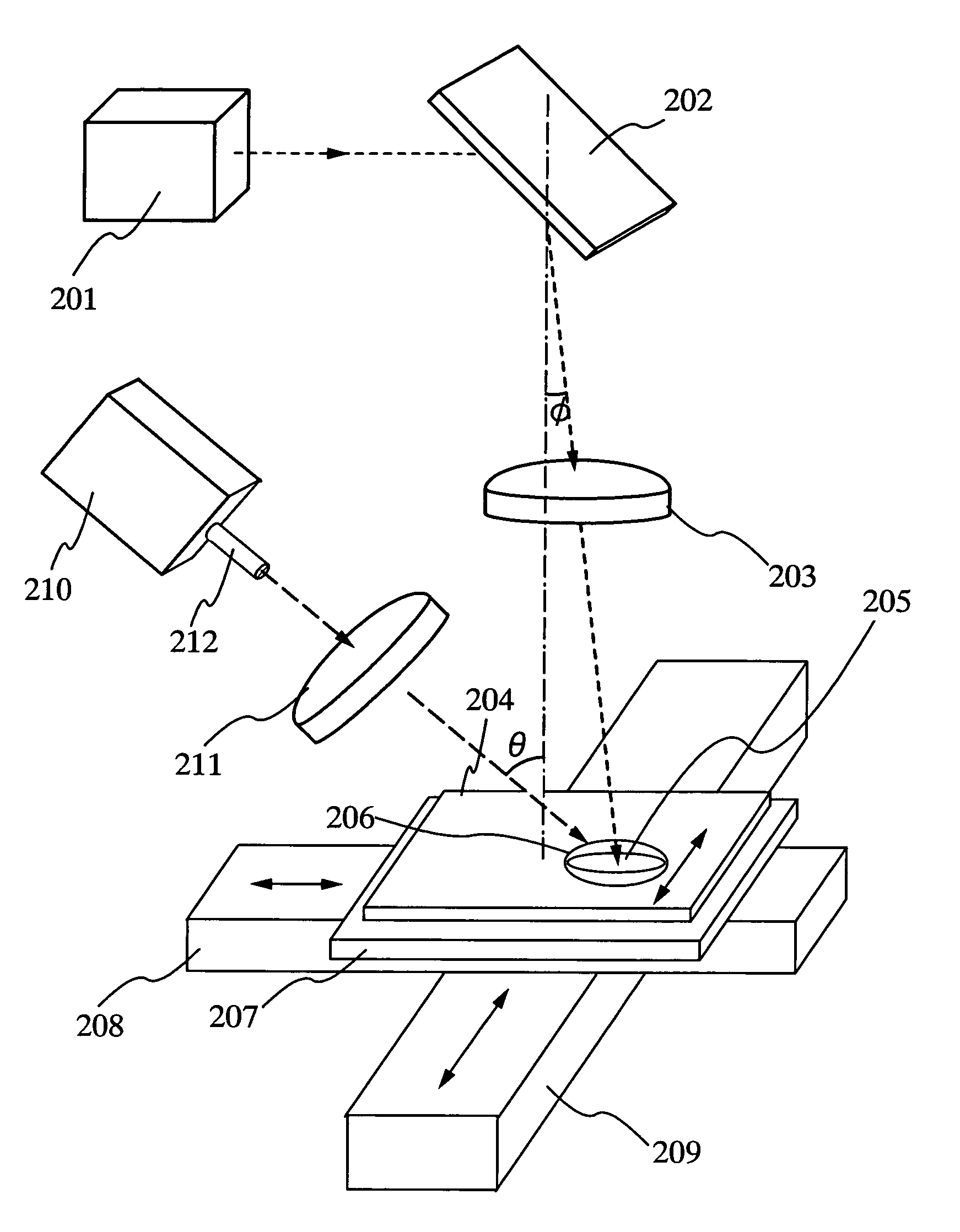
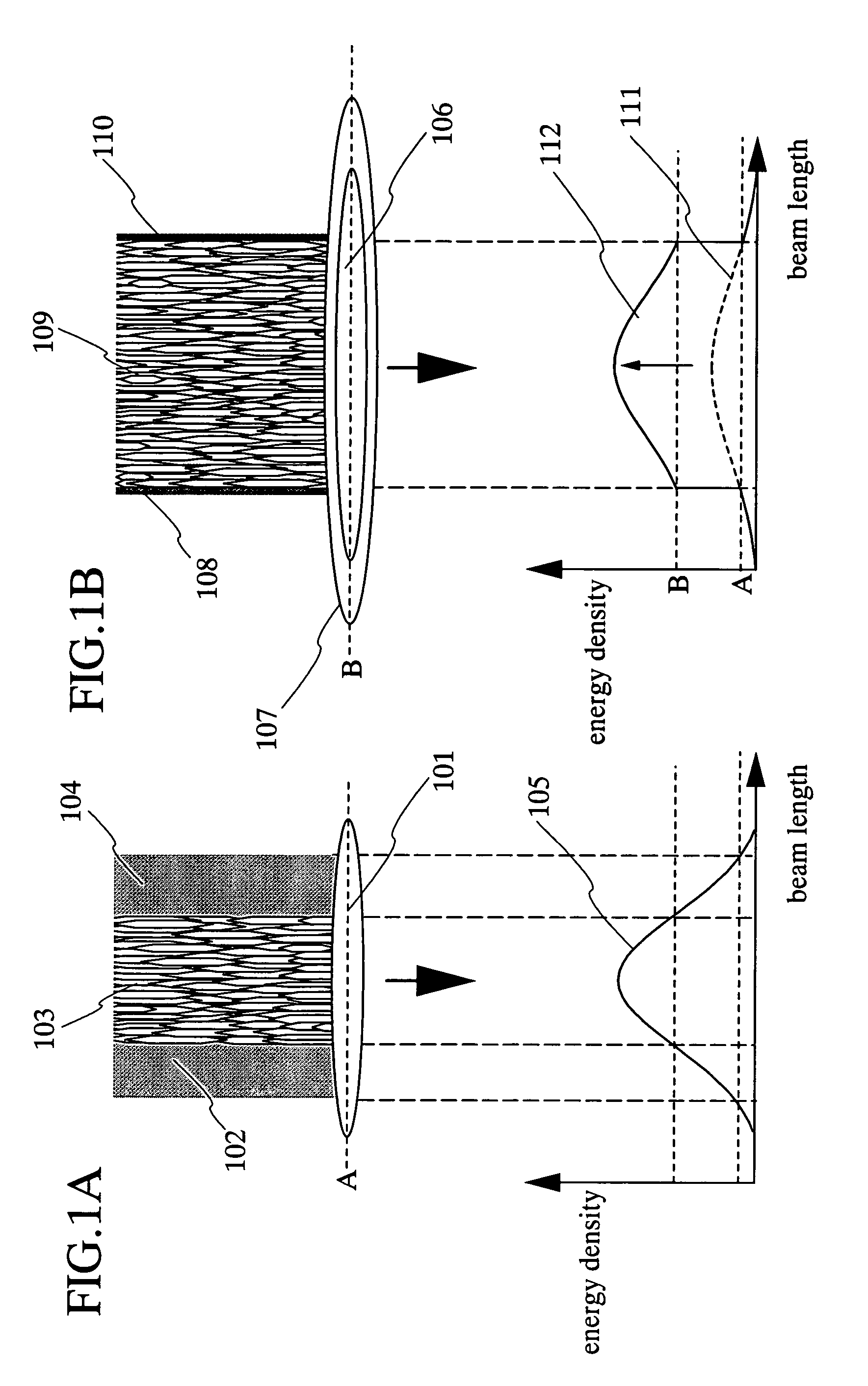
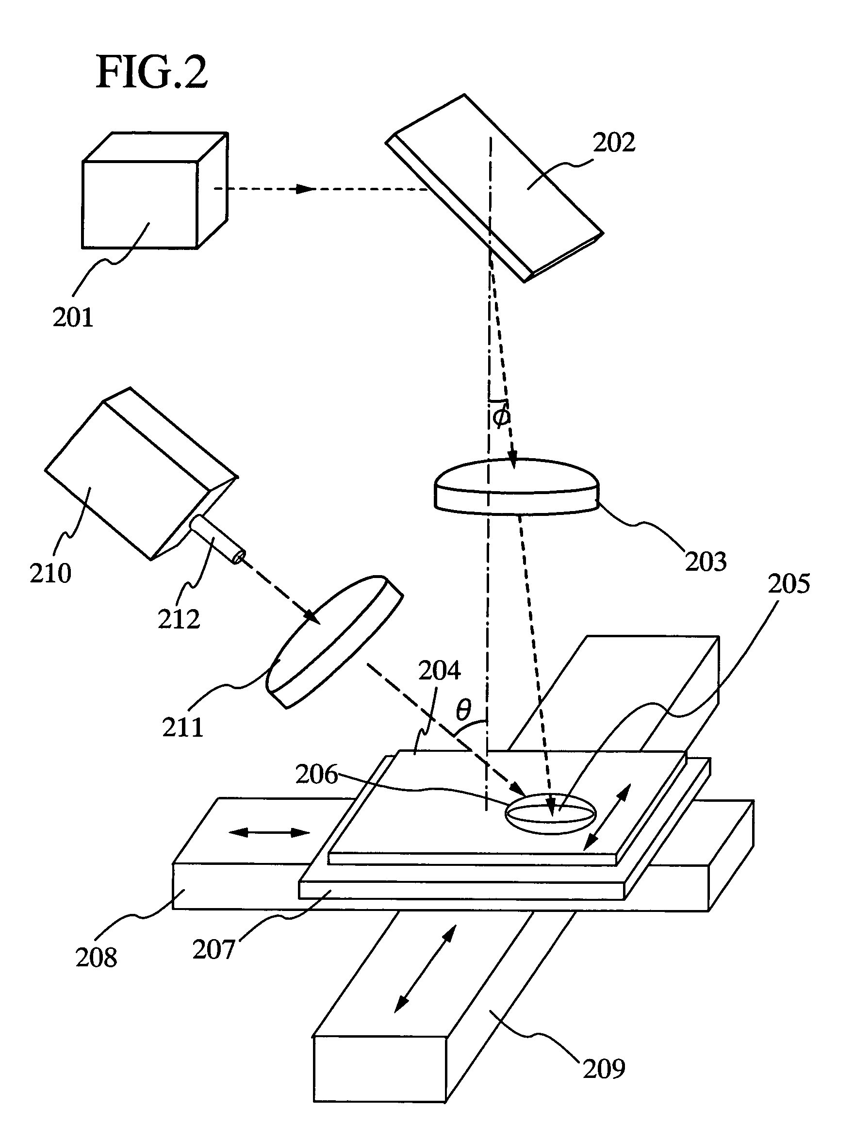
[0064]The embodiment mode 1 of the present invention is explained with reference to FIG. 2. This embodiment mode explains an example in which long beams 205 and 206 are formed to irradiate a surface of a semiconductor film 204.

[0065]First of all, an LD pumped laser oscillator 201 with an output of 10 W (Nd: YVO4 laser, CW, the second harmonic (532 nm)) is prepared. The laser oscillator 201 generates in TEM00 mode, and includes LBO crystal in its resonator to convert the laser beam into the second harmonic. The harmonic is not limited to the second harmonic but the second harmonic is superior to the other higher harmonics in terms of the conversion efficiency. The beam diameter is 2.25 mm. The divergence angle is approximately 0.3 mrad. The traveling direction of the laser beam is changed by a 45° reflecting mirror 202 so as to have an angle of φ from the vertical direction. Next, the laser beam is made incident at an angle φ into a planoconvex lens 203 having a focal length of 20 mm...

embodiment mode 2

[0074]This embodiment mode explains with FIGS. 4A and 4B an example to make the energy distribution of the long beam obtained by shaping the second harmonic shown in embodiment mode 1 more uniform with the fundamental wave.

[0075]First, an LD pumped laser oscillator 301 with an output of 10 W (Nd: YVO4 laser, CW, the second harmonic (532 nm)) is prepared. The laser oscillator 301 generates in TEM00 mode, and includes LBO crystal in its resonator to convert the laser beam into the second harmonic. The beam diameter is 2.25 mm. The divergence angle is approximately 0.3 mrad. The traveling direction of the laser beam is changed by a 45° reflecting mirror 302 so as to have an angle φ from the vertical direction. Next, the laser beam is made incident at an angle φ into a planoconvex lens 303 having a focal length of 20 mm whose plane portion corresponds to a horizontal plane. The angle φ may be changed accordingly, and it is set to 20° in this embodiment mode. The semiconductor film 304 i...

embodiment mode 3

[0082]This embodiment mode explains an example in which several long beams obtained by shaping the second harmonics are combined to form a longer beam, and moreover, it is aided with the energy of the fundamental wave with FIGS. 6A and 6B.

[0083]First, four LD pumped laser oscillators (not shown in the figure) with an output of 10 W (Nd: YVO4 laser, CW, the second harmonic (532 nm)) are prepared. The laser oscillators generate in TEM00 mode and the laser beams emitted from these laser oscillators are converted into the second harmonics through LBO crystal included in their resonators. The beam diameter is 2.25 mm. The divergence angle is 0.3 mrad approximately. Several reflecting mirrors are used in order to change traveling directions of the respective laser beams so as to have an angle β to the vertical direction, and the laser beams are made incident into a surface to be irradiated from four directions so as to be combined into nearly one at the surface to be irradiated. The four ...


PUM

PropertyMeasurementUnit
diameteraaaaaaaaaa
wavelengthaaaaaaaaaa
refractive indexaaaaaaaaaa

Abstract

When the CW laser oscillator is employed in the manufacturing process of the semiconductor device, it is expected to obtain the device of high performance. However, the CW oscillator provides only a small beam spot and forms an inferior crystalline region when it is scanned on the semiconductor film. It is necessary to minimize such an inferior crystalline region because it gives a problem in terms of high integration of the semiconductor element. In view of the problem, the present invention is to form a long crystalline region as suppressing the formation of the inferior crystalline region by irradiating the fundamental wave with the harmonic supplementarily (refer to FIG. 1). The present invention also includes a constitution in which a part having high energy density in the fundamental wave is irradiated to a part having low energy density in the harmonic.

Description

BACKGROUND OF THE INVENTION[0001]1. Field of the Invention[0002]The present invention relates to a laser irradiation method and a laser irradiation apparatus for performing the laser irradiation (the laser irradiation apparatus includes a laser oscillator and an optical system to guide a laser beam emitted from the laser oscillator to an object to be irradiated). In addition, the present invention relates to a method for manufacturing a semiconductor device comprising a step of the laser irradiation process. It is noted that the semiconductor device described here includes a general device that can be operated by utilizing the semiconductor characteristic. And thereby an electro-optical device such as a liquid crystal display device, a light-emitting device or the like, and an electronic device having such an electro-optical device as its component are also included in the semiconductor device.[0003]2. Description of the Related Art[0004]In recent years, the technology to form a thi...

Claims


Application Information

Patent Timeline
Patent Type & Authority Patents(United States)
IPC IPC(8): H01L21/00H01L21/20H01L21/26H01L21/36H01L21/84H01L21/268B23K26/00B23K26/06H01L21/324H01L21/336H01L21/77H01S3/00H01S3/17
CPCB23K26/0732B23K26/0736H01L27/1285H01L21/2026H01S3/005H01L21/02683H01L21/02488H01L21/02678H01L21/02422H01L21/02532H01L21/02595H01L21/02691H01L21/268H01L21/324
Inventor TANAKA, KOICHIROYAMAZAKI, SHUNPEI
Owner SEMICON ENERGY LAB CO LTD
Why Eureka
Try Eureka