
Random number generating method and semiconductor integrated circuit device

a technology of integrated circuits and random numbers, which is applied in the field of random number generating methods and semiconductor integrated circuit devices, can solve the problems of difficult to guarantee the quality of random numbers, complicated circuits and elements which cannot be obtained in a simple device, and the good and bad points of conventional random number generating circuits, so as to achieve small area and reduce power consumption

Inactive Publication Date: 2010-04-20
HITACHI ULSI SYST CO LTD
View PDF21 Cites 10 Cited by
  • Summary
  • Abstract
  • Description
  • Claims
  • Application Information

AI Technical Summary

Benefits of technology

"The present invention provides a method for generating a high-quality random number using a small area without requiring modification of the fabrication process. The method includes a plurality of unit circuits and a signal variation detecting circuit. The unit circuits have an identical shape and fabrication process and amplifier circuit for forming a binary signal by amplifying a noise superposed on the differential voltage of threshold voltages of the first and the second logic circuits. The signal variation detecting circuit has an output signal in response to variation in any of a plurality of binary signals outputted from the plurality of unit circuits. The plurality of binary signals outputted from the signal variation detecting circuit are combined to generate a random number. This invention also reduces power consumption and improves the quality of the random number."

Problems solved by technology

However, the conventional random number generating circuits have good and bad points.
True random number has advantages of eventuality, un-reproducibility, and unpredictability but it requires a complicated circuit and element which cannot be obtained in a simple device.
Accordingly, a factor lowering the irregularity of a random number cannot be predicted at the design stage and it is difficult to guarantee the quality of the random number.

Method used


Image

  • Random number generating method and semiconductor integrated circuit device
  • Random number generating method and semiconductor integrated circuit device
  • Random number generating method and semiconductor integrated circuit device

Examples


Embodiment Construction

[0041]The invention will be described in detail with reference to the attached drawings.

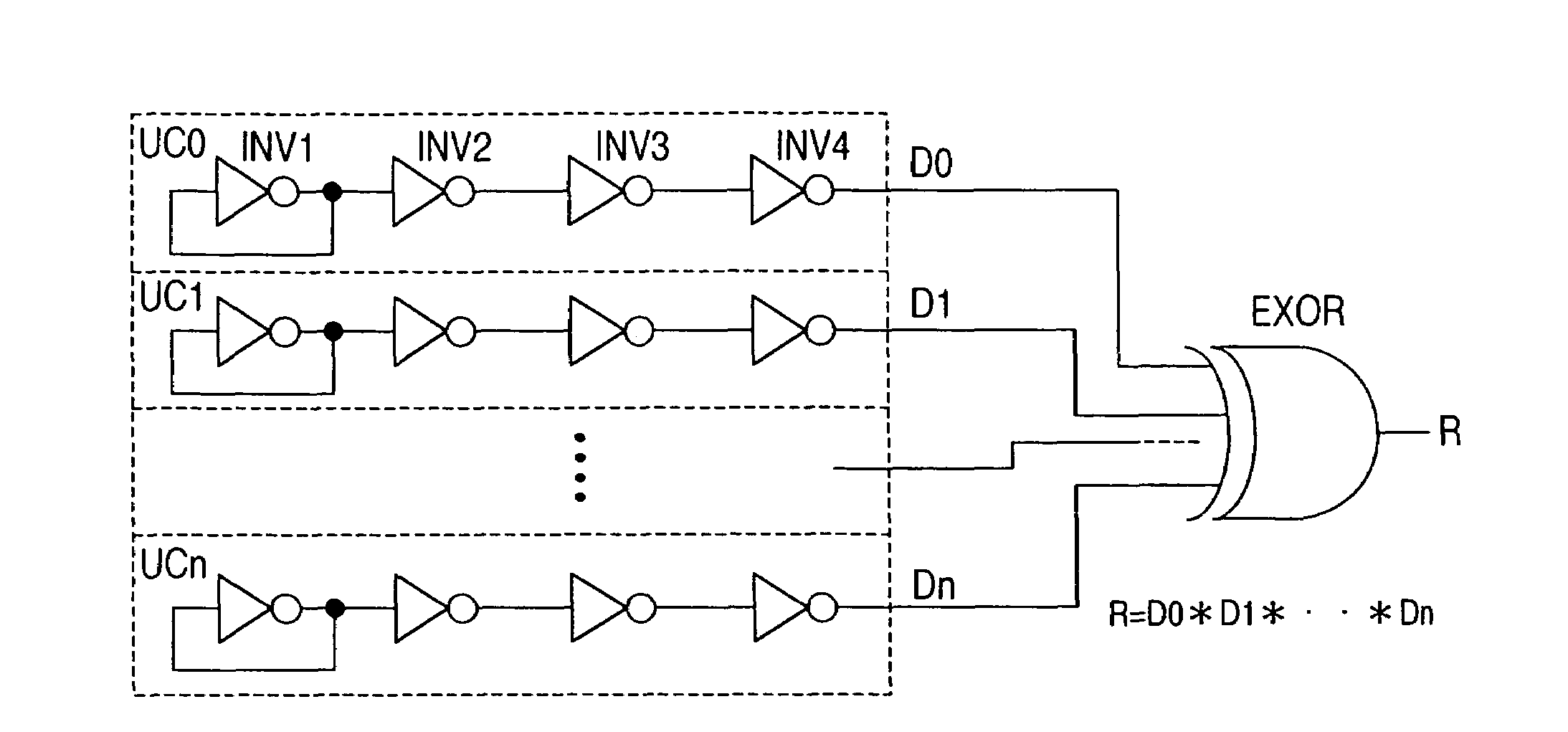
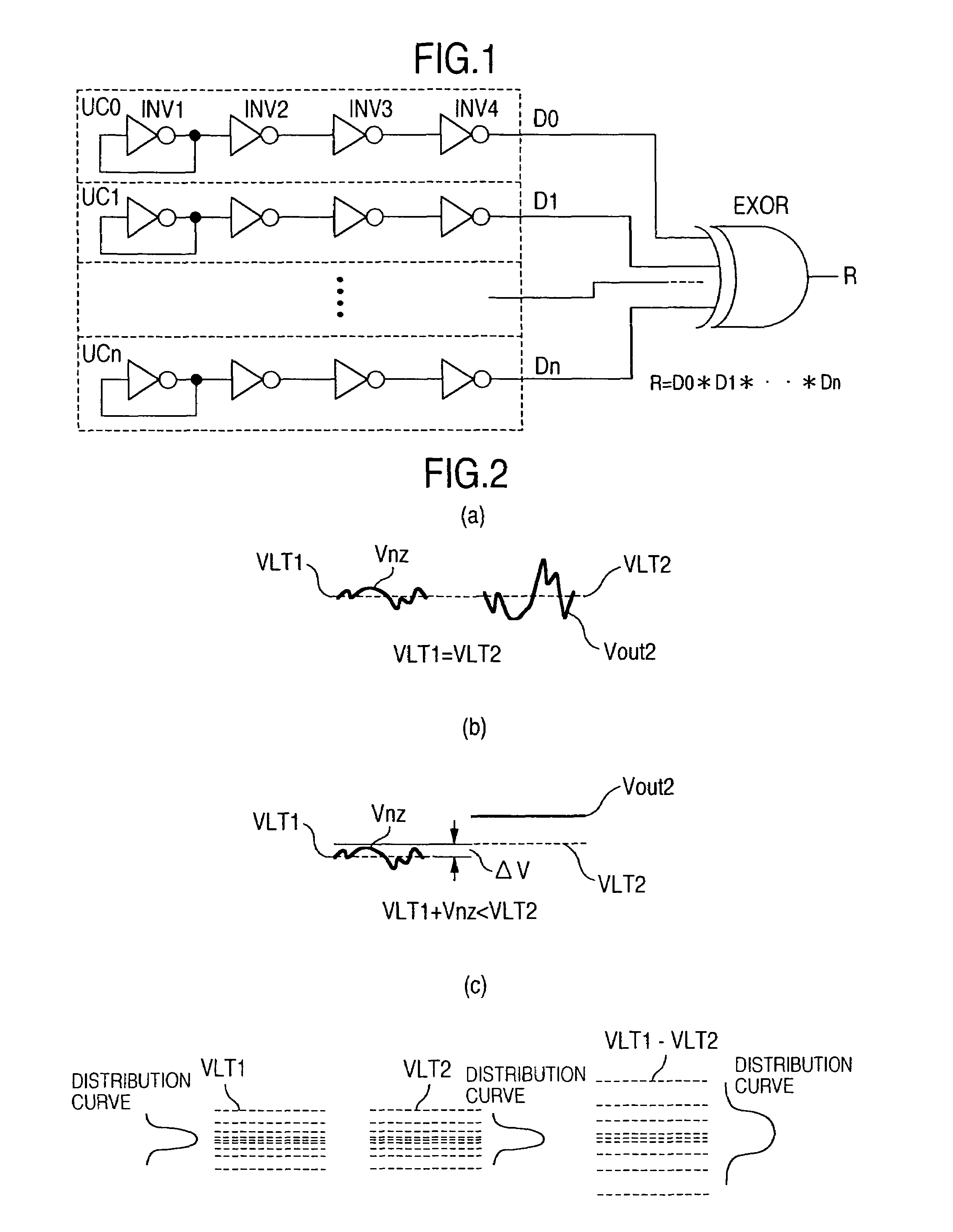
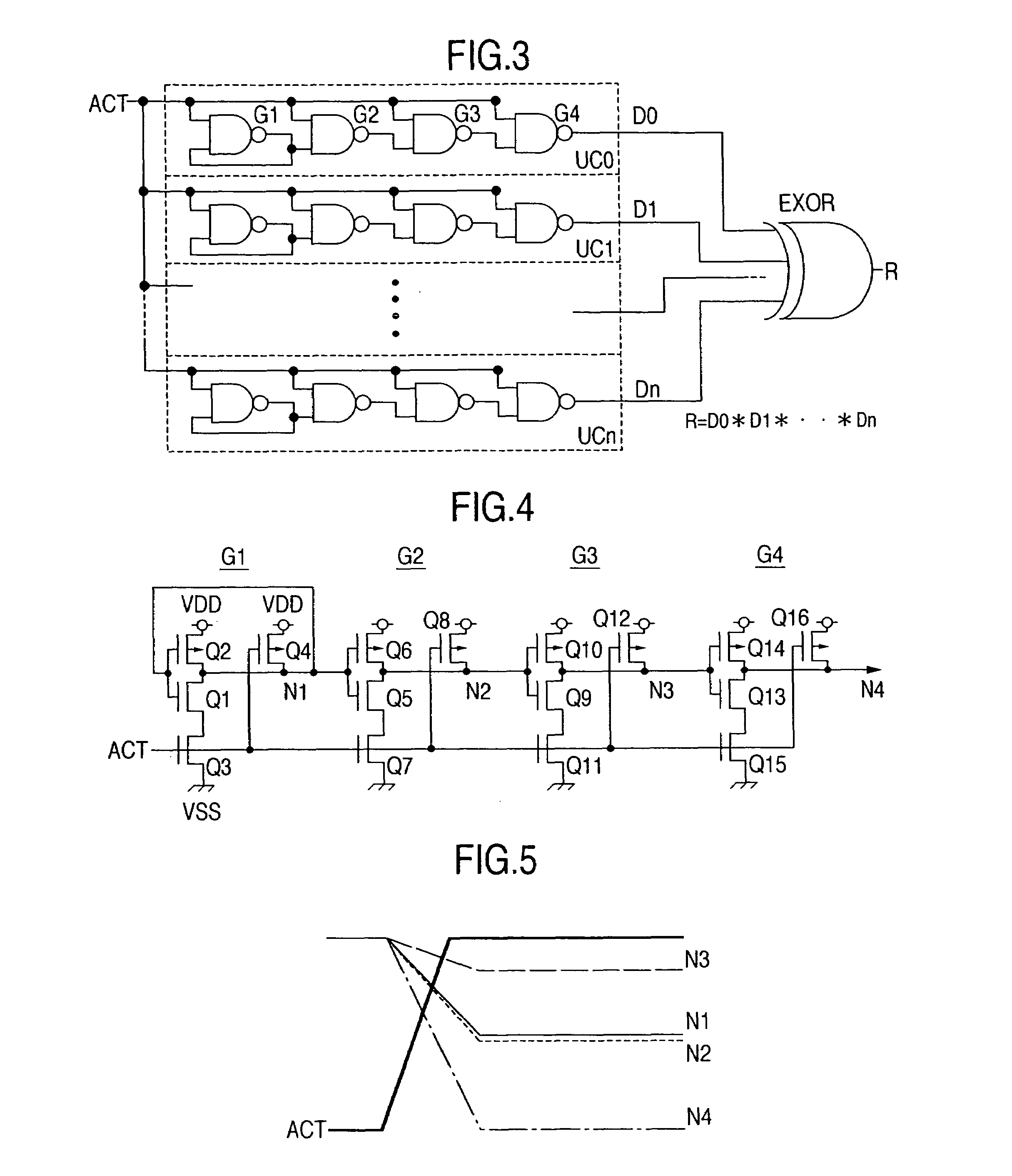
[0042]FIG. 1 shows a circuit diagram of the basic concept of a true random number generating circuit mounted on a semiconductor integrated circuit device according to the present invention. CMOS inverter circuits INV1 to INV4 shown in FIG. 1 are configured so as to have identical characteristic within an actually controllable range according to the design and fabrication of the semiconductor integrated circuit device. The technique for making that a plurality of inverters have identical characteristic will be briefly explained below.

[0043]In a CMOS inverter circuit, it is considered that its characteristic is substantially decided by relative conductance between a P-channel type MOSFET and an N-channel type MOSFET constituting the circuit. In this viewpoint, CMOS inverters of the identical characteristic can be configured by MOSFET having an identical ratio W / L wherein W is the channel width W an...


PUM


Abstract

A random number generating method for an electronic device including a plurality of unit circuits each first and second logic circuits, each logic circuit having a same shape and being formed through a same fabrication process, and an amplifier circuit for forming a binary signal by amplifying a noise superposed on the differential voltage of threshold voltages of the first and the second logic circuits; and a signal variation detecting circuit for forming an output signal in response to a variation in any of a plurality of binary signals outputted from the plurality of unit circuits, wherein a plurality of binary signals outputted from the signal variation detecting circuit are combined to generate a random number.

Description

TECHNICAL FIELD[0001]The present invention relates to a random number generating method and a semiconductor integrated circuit device and in particular, to a random number generating method appropriate for a semiconductor fabrication technique and a technique which can be effectively used in the semiconductor integrated circuit device.BACKGROUND ART[0002]Recently, networks and IT technique are rapidly spread all over the world, which requires security technique such as the encryption technique and the authentication technique. As one element of these techniques, random numbers are often used. Currently, random number generating circuits based on several types of basic principles have come into practical use. “Toshiba Review” Vol. 58.8 (2003) (first prior art) is an example of ultra-small-size true random number generating circuit for sophisticated information security. Moreover, JP-A-2003-173254 (second prior art) discloses a random number generating circuit using an ambiguous outpu...

Claims


Application Information

Patent Timeline
Patent Type & Authority Patents(United States)
IPC IPC(8): G06F1/02G06F7/58
CPCH04L9/06G06F7/588G06F7/58G11C7/06G06F7/57
Inventor MURANAKA, MASAYA
Owner HITACHI ULSI SYST CO LTD
Features
  • Generate Ideas
  • Intellectual Property
  • Life Sciences
  • Materials
  • Tech Scout
  • Unparalleled Data Quality
  • Higher Quality Content
  • 60% Fewer Hallucinations
Learn More