Method for producing a light emitting device
a technology of light-emitting devices and active layers, which is applied in the direction of semiconductor devices, basic electric elements, electrical apparatus, etc., can solve the problems of poor shape reproducibility of the unevenness structure, poor shape reproducibility of the minute unevenness structure, and inability to efficiently extract light emitted from an active layer of a light-emitting device. , to achieve the effect of improving light extraction efficiency, preventing multiple reflection, and improving the structure of the minute unevenness
- Summary
- Abstract
- Description
- Claims
- Application Information
AI Technical Summary
Benefits of technology
Problems solved by technology
Method used
Image
Examples
first embodiment
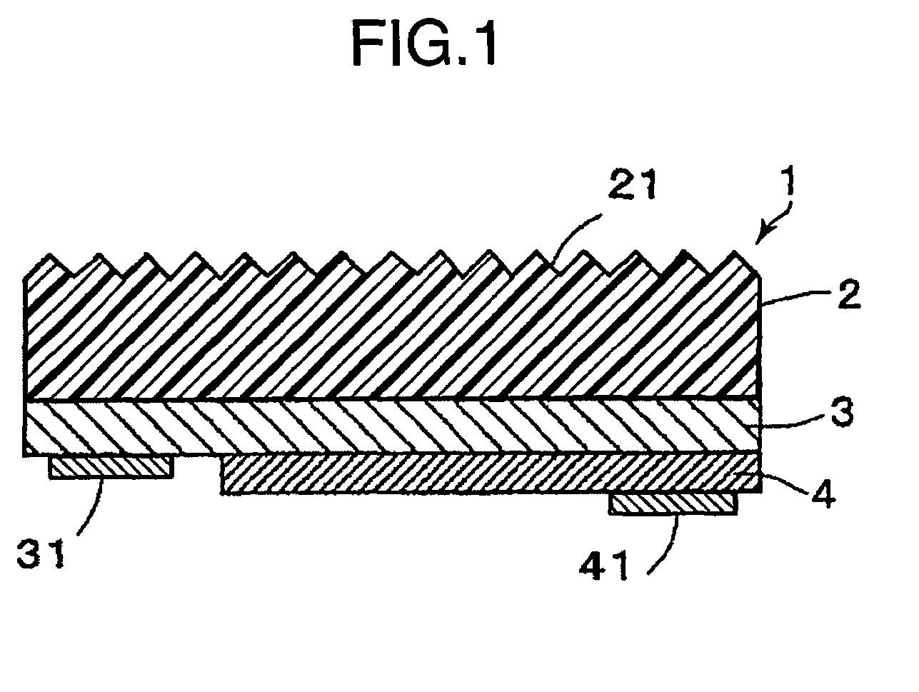
[0047]First, with respect to FIGS. 4A to 4F, a process for producing the light-emitting device 1 by the production method of the first embodiment is described.
[0048]As shown in FIG. 4A, one or more light-emitting devices are formed by adhering the light-emitting layer comprised of the semiconductor layers 3, 4 to one surface (lower surface in FIG. 4A) of one transparent crystal substrate 2 made of, e.g., sapphire (Al2O3). In the case of charging the transparent crystal substrate 2 with a function of the bearing layer having a thickness capable of being handled at the time of mounting the light-emitting device and an optical function, the minute unevenness structure 21 for preventing the multiple reflection are formed on the other surface (upper surface in FIG. 4A) of the transparent crystal substrate 2.
[0049]As shown in FIG. 4B, a resist (e.g., PMMA: methacrylic resin, Novolac resist) as a material of a transfer layer 5 is so spin-coated on the other surface of the transparent cryst...
second embodiment
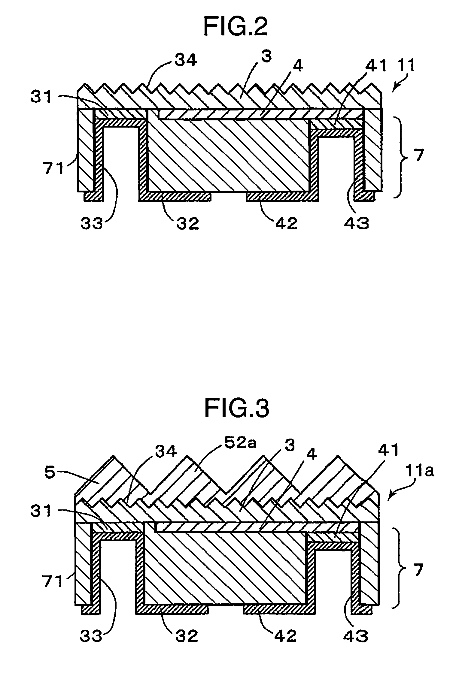
[0093]Next, the production process of the light-emitting device 11 by the production method of the second embodiment is described with reference to FIGS. 11A to 11I.
[0094]The light-emitting device 11 shown in FIG. 11 is constructed such that a light-emitting layer comprised of an n-type GaN semiconductor layer 3 and a p-type GaN semiconductor layers 4 is adhered to one surface (lower surface in FIG. 11) of the transparent crystal substrate 2 made of, e.g., sapphire (Al2O3). As shown in FIG. 11B, a resin coated copper (RCC) 70 including a resin layer 71 and a copper foil 72 is adhered to the outer surfaces of the semiconductor layers 3, 4. Thereafter, VIA formation, patterning, plating and the like which are ordinary printed circuit board processing steps are applied to the resin coated copper 70, thereby forming a light-emitting device provided with a substrate bearing layer 7 as shown in FIG. 11C.
[0095]The substrate bearing layer 7 includes the resin layer 71 for bearing the semico...
PUM
 Abstract
Description
Claims
Application Information


