Advanced multilayer dielectric cap with improved mechanical and electrical properties

a dielectric cap and multi-layer technology, applied in the direction of basic electric elements, material analysis, instruments, etc., can solve the problems of reducing the size of the device to nanometer dimensions, adhesion problems, and the metallurgical requirements no longer meet requirements, so as to reduce the impact of uv cure, reduce the stress of the film, and increase the optical band gap

Inactive Publication Date: 2010-06-15
ADVANCED MICRO DEVICES INC +2
View PDF5 Cites 22 Cited by
  • Summary
  • Abstract
  • Description
  • Claims
  • Application Information

AI Technical Summary

Benefits of technology

[0013]More particularly, the present invention provides a dielectric cap including multilayers of dielectric materials, wherein at least one of the multilayers provides good oxidation resistance, inhibits Cu diffusion and / or provides substantially high mechanical stability for the multilayer cap-interlevel dielectric structures by maintaining the compressive stress value under UV and / or E-beam radiation during a post-deposition curing process.
[0015]The inventive dielectric cap exhibits a high compressive stress (equal to, or greater than, 150 MPa as-deposited) and high modulus (on the order of 20 GPa or greater) and maintains the compressive stress and modulus values after a post-deposition curing treatment process. When the inventive dielectric cap is used in an advanced interconnect structure, such as for example, a Cu-containing low k BEOL nanoelectric structure, little or no film and device cracking is observed as compared to an interconnect structure including a conventional dielectric cap. Moreover, the use of the inventive dielectric cap in an advanced interconnect structure improves the reliability of the interconnect structure as compared to a prior art interconnect structure including a conventional dielectric cap.
[0022]In a still further embodiment of the first aspect of the present invention, the inventive dielectric cap further includes another layer which includes atoms of at least Si and C, optionally O, wherein the C atoms are present in an amount of about 15 atomic % or greater, preferably from about 20 to about 35 atomic %, to provide a layer within the multilayered dielectric material stack that improves the etch selectivity of the dielectric cap to the interlevel or intralevel dielectric.
[0030]In another embodiment of the second aspect of the present invention, the Si—N bonding within the inventive dielectric cap is of a sufficient content to provide a dielectric cap with high optical band gap (on the order of about 3.0 EV (electron-volts) or greater) layer which substantially blocks UV radiation during a post deposition UV curing process. This will minimize the impact of UV cure in the bottom layer of the multilayer structure and reduce the change in the film's stress by post UV cure.
[0031]In a further embodiment of the second aspect of the present invention, another layer is present which includes atoms of at least Si and C wherein said C atoms are present in an amount of about 15 atomic % or greater so as to provide a layer within the mutilayered dielectric material stack that improves the etch selectivity of the dielectric cap to the interlevel or intralevel dielectric.
[0035]A yet still further embodiment of the present invention, the inventive dielectric cap includes an oxygen diffusion barrier overlayer located atop a lower layer having the Si—N bonding mentioned above. This will act as an additional oxidation barrier and specific plasma etch selectivity where etching chemistry is more selective to Si—N bonding. In some embodiments, the oxygen diffusion barrier overlayer is formed by contacting the lower layer having the Si—N bonding with oxygen at an elevated temperature (greater than about 120° C.). In this embodiment, the layer including the Si—N bonding has a bonding matrix of Si—N, N—Si—C, or Si—N—C. When exposed to oxygen, the layer including one of the aforementioned bonding matrix forms an oxygen diffusion barrier surface layer that has one of the following bonding matrixes Si—N—O, N—Si—C—O or O—Si—N—C. Basically, the bottom oxidation barrier properties of the bottom layer can be improved by a brief oxidation to form an intermediate oxygen bearing interface prior to the deposition of higher carbon contained low-k top layer of the dielectric cap.

Problems solved by technology

While Al-based metallurgies have been the material of choice for use as metal interconnects in the past, Al-based metallurgies no longer satisfy requirements as circuit density and speeds for IC chips increase and the scale of the devices decreases to nanometer dimensions.
One challenge relative to using Cu-based (i.e., pure Cu and Cu alloys) metallurgy is that it diffuses readily into the surrounding interconnect dielectric material as BEOL processing steps continue.
Typically, the energy of the curing process such as, for example, UV exposure, changes the stress of the cap layer from compressive to tensile which could potentially result in cracking and adhesion problems in both the cap layer and the ULK dielectric material, Any crack in the cap layer may lead to copper diffusion into the interconnect dielectric material layer, i.e., ILD, through the seam leading to formation of a copper nodule under the cap layer.
The presence of such a copper nodule in the ILD may lead to short circuits due to leakage of current between adjacent interconnect lines.
The change from the cap film's compressive to tensile stress during the post-deposition curing treatment process will create intrinsic mechanically instability between the metal-cap-dielectric films and may also cause other damages such as, for example, increased cap-interlevel dielectric film cracking, delamination and blister formation over patterned copper lines, particularly during subsequent dielectric depositions, metallization, and chemical-mechanical polishing.

Method used


Image

  • Advanced multilayer dielectric cap with improved mechanical and electrical properties
  • Advanced multilayer dielectric cap with improved mechanical and electrical properties

Examples


Embodiment Construction

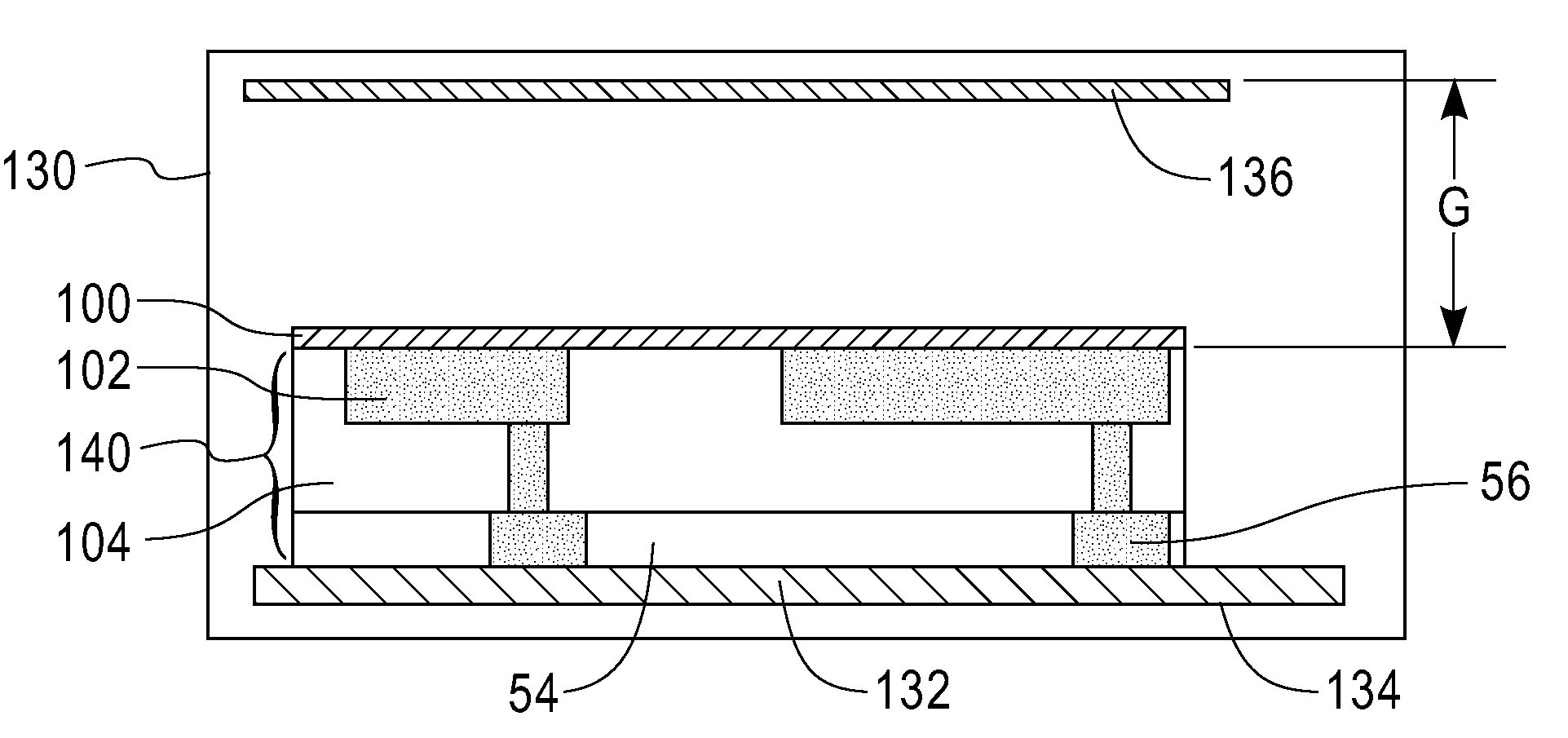
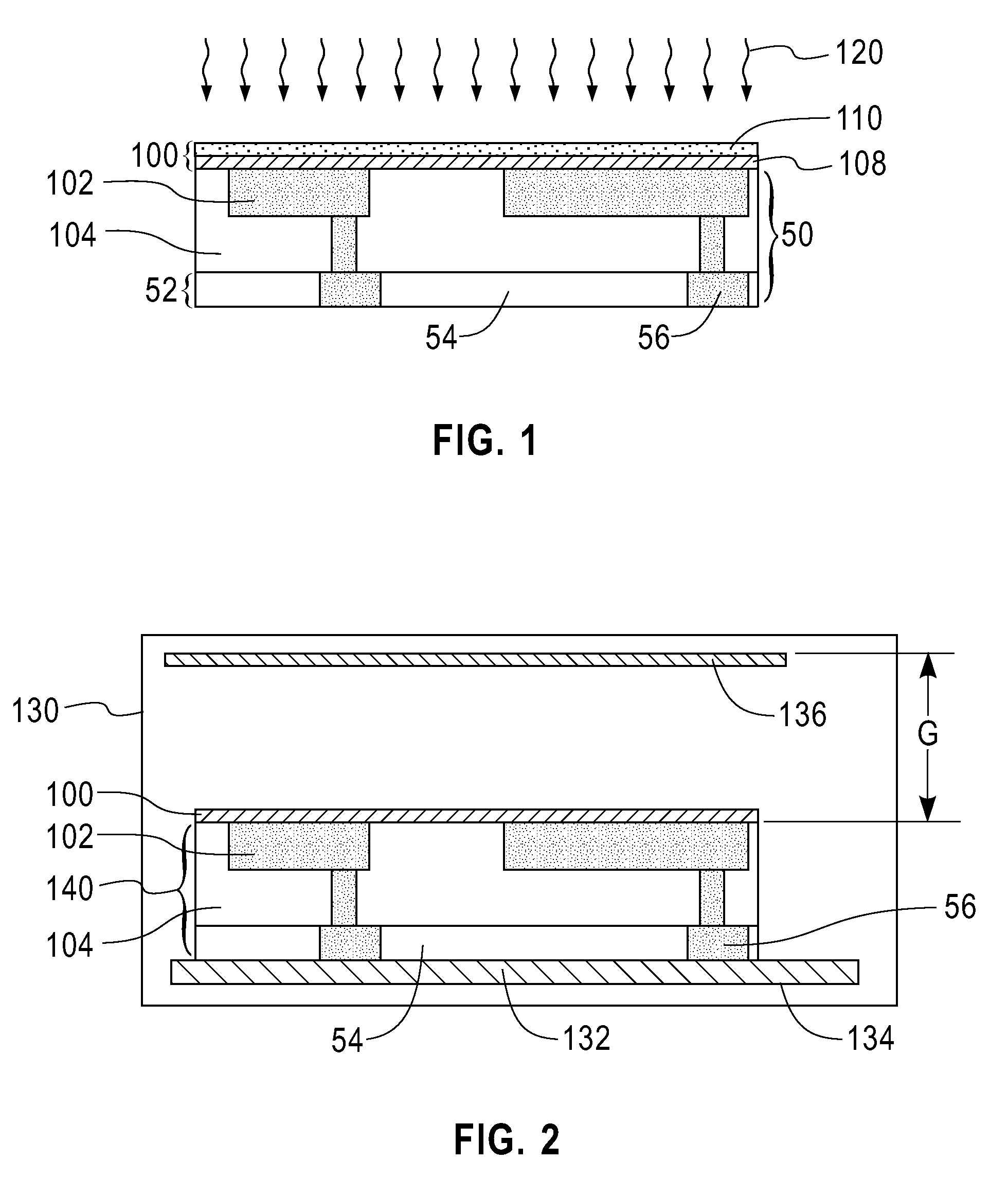
[0049]The present invention, which provides a dielectric cap, an interconnect structure including the inventive dielectric cap located above an interlevel or intralevel dielectric having at least one conductive material embedded therein and related methods of forming the dielectric cap and the interconnect structure, will now be described in greater detail by referring to the following discussion and drawings that accompany the present application. It is noted that the drawings of the present application are provided for illustrative purposes only and, as such, the drawings are not drawn to scale.

[0050]In the following description, numerous specific details are set forth, such as particular structures, components, materials, dimensions, processing steps and techniques, in order to provide a thorough understanding of the present invention. However, it will be appreciated by one of ordinary skill in the art that the invention may be practiced without these specific details. In other i...


PUM

PropertyMeasurementUnit
compressive stressaaaaaaaaaa
optical band gapaaaaaaaaaa
compressive stressaaaaaaaaaa

Abstract

A dielectric cap, interconnect structure containing the same and related methods are disclosed. The inventive dielectric cap includes a multilayered dielectric material stack wherein at least one layer of the stack has good oxidation resistance, Cu diffusion and / or substantially higher mechanical stability during a post-deposition curing treatment, and including Si—N bonds at the interface of a conductive material such as, for example, Cu. The dielectric cap exhibits a high compressive stress and high modulus and is still remain compressive stress under post-deposition curing treatments for, for example: copper low k back-end-of-line (BEOL) nanoelectronic devices, leading to less film and device cracking and improved reliability.

Description

FIELD OF THE INVENTION[0001]The present invention relates generally to integrated circuit (IC) chip fabrication, and more particularly, to a dielectric cap for an advanced interconnect structure, such as, for example, a copper-containing ultra-low dielectric constant dielectric interconnect structure.BACKGROUND OF THE INVENTION[0002]In traditional IC chips, aluminum, Al, and aluminum alloys have been used as interconnect metallurgies for providing electrical connections to and from devices in semiconductor interconnect (i.e., back-end-of-the-line, BEOL) layers of the devices. While Al-based metallurgies have been the material of choice for use as metal interconnects in the past, Al-based metallurgies no longer satisfy requirements as circuit density and speeds for IC chips increase and the scale of the devices decreases to nanometer dimensions. Thus, copper, Cu, and Cu-alloys are being employed as a replacement for Al-based metallurgies in nano-electronic devices because of their lo...

Claims


Application Information

Patent Timeline
Patent Type & Authority Patents(United States)
IPC IPC(8): H01L21/31H01L21/469H01L23/48H01L23/58
CPCG01N33/56972G01N2800/24G01N2800/042G01N2333/7051H01L21/02348H01L21/76832H01L21/76834
Inventor BHATIA, RITWIKBONILLA, GRISELDAGRILL, ALFREDHERMAN, JOSHUA L.NGUYEN, SON VANRYAN, E. TODDSHOBHA, HOSADURGA
Owner ADVANCED MICRO DEVICES INC
Why Eureka
Try Eureka