Single-photon detector with a quantum dot and a nano-injector

a quantum dot and detector technology, applied in semiconductor devices, diodes, electrical apparatus, etc., can solve the problems of high internal noise, inability to detect single photo-generated electrons with conventional electronic circuits, and inability to detect single photo-generated electrons with conventional electronic circuits, and achieve the effect of increasing the rate of injected carriers

a quantum dot and detector technology, applied in semiconductor devices, diodes, electrical apparatus, etc., can solve the problems of high internal noise, inability to detect single photo-generated electrons with conventional electronic circuits, and inability to detect single photo-generated electrons with conventional electronic circuits, and achieve the effect of increasing the rate of injected carriers

US7745816B2Active Publication Date: 2010-06-29NORTHWESTERN UNIV

Image

  • Single-photon detector with a quantum dot and a nano-injector
  • Single-photon detector with a quantum dot and a nano-injector
  • Single-photon detector with a quantum dot and a nano-injector

Examples


Embodiment Construction

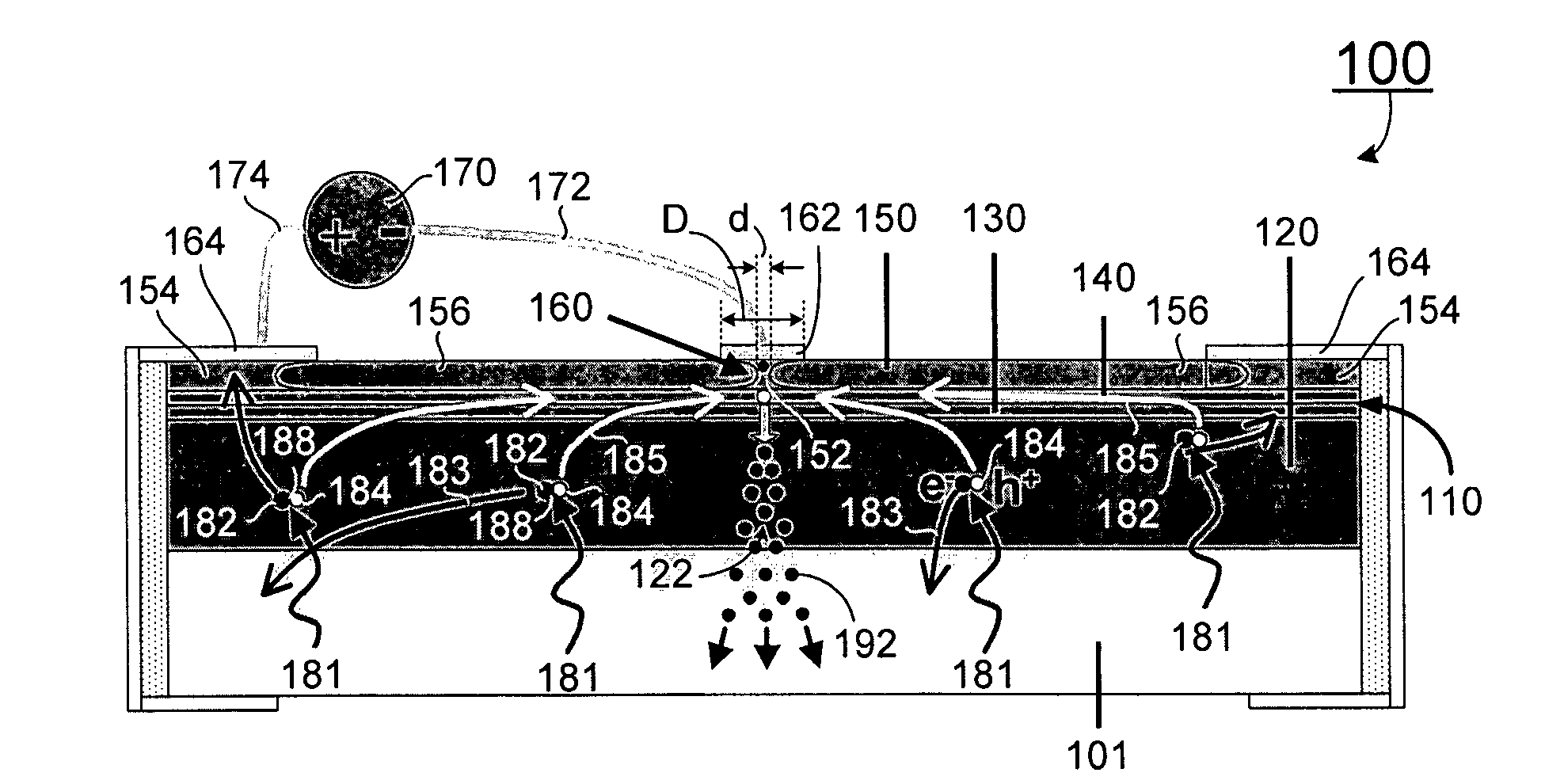
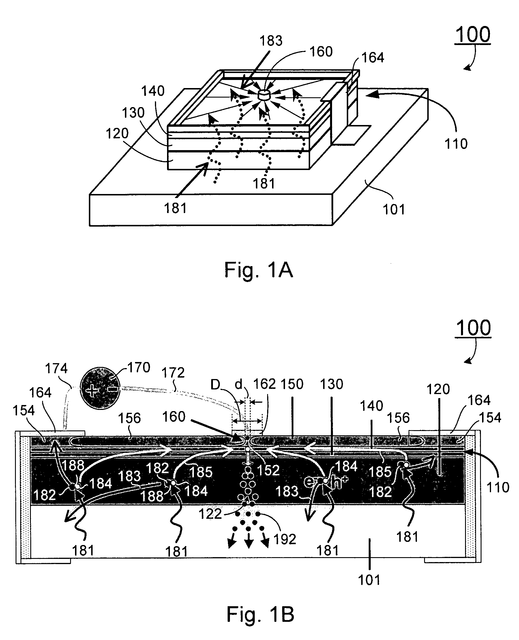
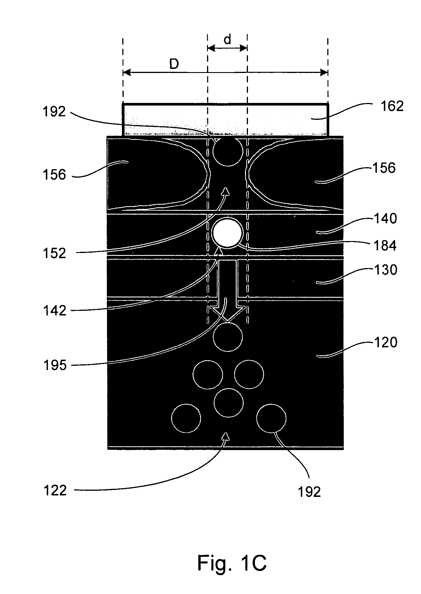
[0055]The present invention is more particularly described in the following examples that are intended as illustrative only since numerous modifications and variations therein will be apparent to those skilled in the art. Various embodiments of the invention are now described in detail. Referring to the drawings, like numbers indicate like parts throughout the views. As used in the description herein and throughout the claims that follow, the meaning of “a,”“an,” and “the” includes plural reference unless the context clearly dictates otherwise. Also, as used in the description herein and throughout the claims that follow, the meaning of “in” includes “in” and “on” unless the context clearly dictates otherwise. Moreover, titles or subtitles may be used in the specification for the convenience of a reader, which has no influence on the scope of the invention. Additionally, some terms used in this specification are more specifically defined below.

DEFINITIONS

[0056]The terms used in this...


PUM


Abstract

A semiconductor photodetector for photon detection without the use of avalanche multiplication, and capable of operating at low bias voltage and without excess noise. In one embodiment, the photodetector comprises a plurality of InP / AlInGaAs / AlGaAsSb layers, capable of spatially separating the electron and the hole of an photo-generated electron-hole pair in one layer, transporting one of the electron and the hole of the photo-generated electron-hole pair into another layer, focalizing it into a desired volume and trapping it therein, the desired volume having a dimension in a scale of nanometers to reduce its capacitance and increase the change of potential for a trapped carrier, and a nano-injector, capable of injecting carriers into the plurality of InP / AlInGaAs / AlGaAsSb layers, where the carrier transit time in the nano-injector is much shorter than the carrier recombination time therein, thereby causing a very large carrier recycling effect.

Description

CROSS-REFERENCE TO RELATED PATENT APPLICATION[0001]This application claims the benefit, pursuant to 35 U.S.C. §119(e), of U.S. provisional patent application Ser. No. 60 / 721,007, filed Sep. 27, 2005, entitled “focalized carrier augmented sensors for single photon detection,” by Hooman Mohseni, which is incorporated herein by reference in its entirety.[0002]Some references, which may include patents, patent applications and various publications, are cited and discussed in the description of this invention. The citation and / or discussion of such references is provided merely to clarify the description of the present invention and is not an admission that any such reference is “prior art” to the invention described herein. All references cited and discussed in this specification are incorporated herein by reference in their entireties and to the same extent as if each reference was individually incorporated by reference. In terms of notation, hereinafter, “[n]” represents the nth refer...

Claims


Application Information

Patent Timeline
29 Jun 2010
Publication
US7745816B2
IPC
H01L29/06; H01L31/00; H01L29/08
CPC
H01L27/14643
Inventors
MOHSENI, HOOMAN