

Dielectric substrate with reflecting films
a dielectric substrate and film technology, applied in the direction of semiconductor devices, electrical equipment, radio frequency controlled devices, etc., can solve the problems of sapphire substrate warping, sapphire substrate formation cracks, time-consuming and therefore expensive process of forming a polysilicon layer at least about 2 m thick, etc., to improve the crystalline structure of silicon oxid
- Summary
- Abstract
- Description
- Claims
- Application Information
AI Technical Summary
Benefits of technology
Problems solved by technology
Method used
Image

Examples
first embodiment
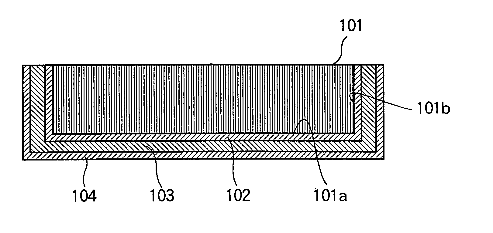
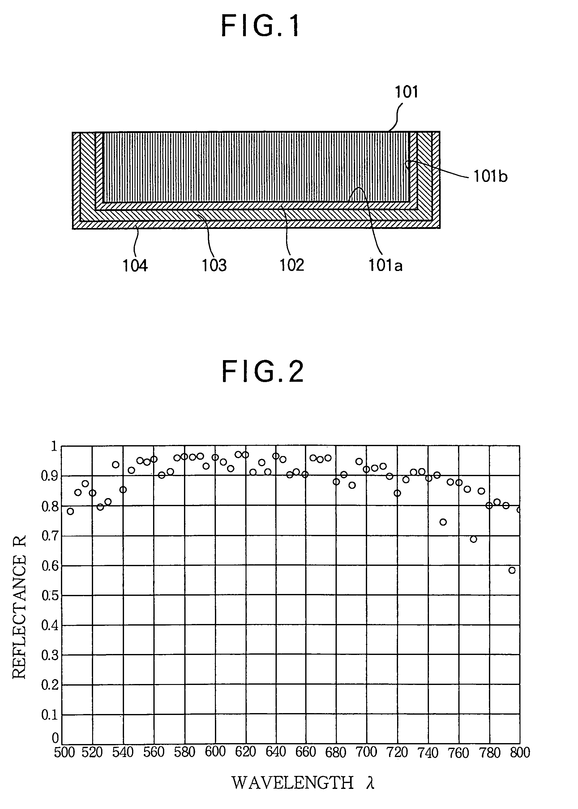
[0047]Referring to FIG. 1, the first embodiment is a semiconductor device or wafer having a silicon-on-sapphire (SOS) substrate 101, the major surfaces of which are a front surface and a back surface 101a. The back surface 101a and side surfaces 101b of the SOS substrate 101 are covered with reflective films 102, 103, 104 to permit optical sensing by wafer sensing light. The second reflective film 103 has a lower refractive index than the first and third reflective films 102, 104. The first reflective film 102 is, for example, a polysilicon film formed on the back and side surfaces of the SOS substrate 101. The second reflective film 103 is, for example, a silicon oxide film formed on the first reflective film 102. The third reflective film 104 is, for example, a polysilicon film formed on the second reflective film 103.
[0048]Next the determination of the film thicknesses of the reflective films will be described.
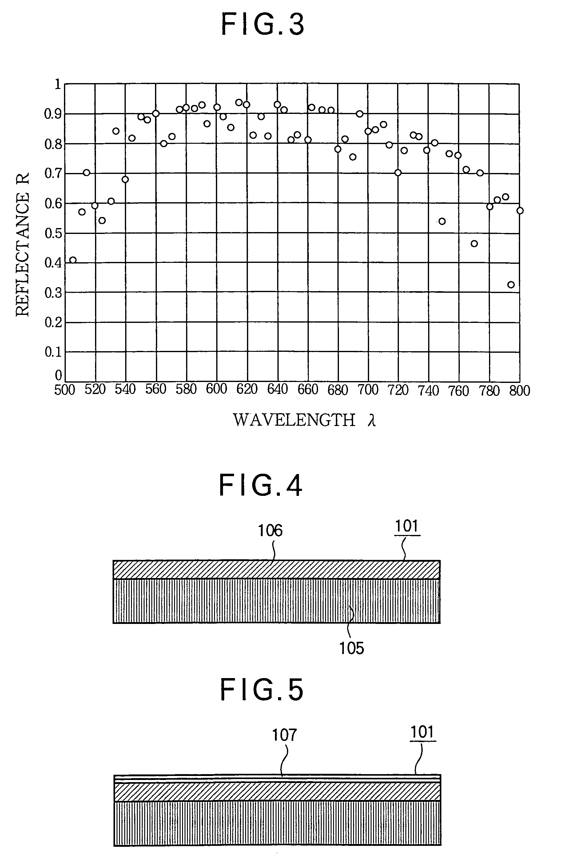
[0049]Let the refractive index of the space through which the wafer se...
PUM
| Property | Measurement | Unit |
|---|---|---|
| thickness | aaaaa | aaaaa |
| thickness | aaaaa | aaaaa |
| thickness | aaaaa | aaaaa |
Abstract
Description
Claims
Application Information