Two-layer film for next generation damascene barrier application with good oxidation resistance

a damascene barrier and two-layer film technology, applied in the direction of chemical vapor deposition coating, coating,plasma technique, etc., can solve the problems of copper being difficult to etch and achieve precise patterns, forming short circuits, and forming short circuits

a damascene barrier and two-layer film technology, applied in the direction of chemical vapor deposition coating, coating,plasma technique, etc., can solve the problems of copper being difficult to etch and achieve precise patterns, forming short circuits, and forming short circuits

US7749563B2Inactive Publication Date: 2010-07-06APPLIED MATERIALS INC

Image

  • Two-layer film for next generation damascene barrier application with good oxidation resistance
  • Two-layer film for next generation damascene barrier application with good oxidation resistance
  • Two-layer film for next generation damascene barrier application with good oxidation resistance

Examples


examples

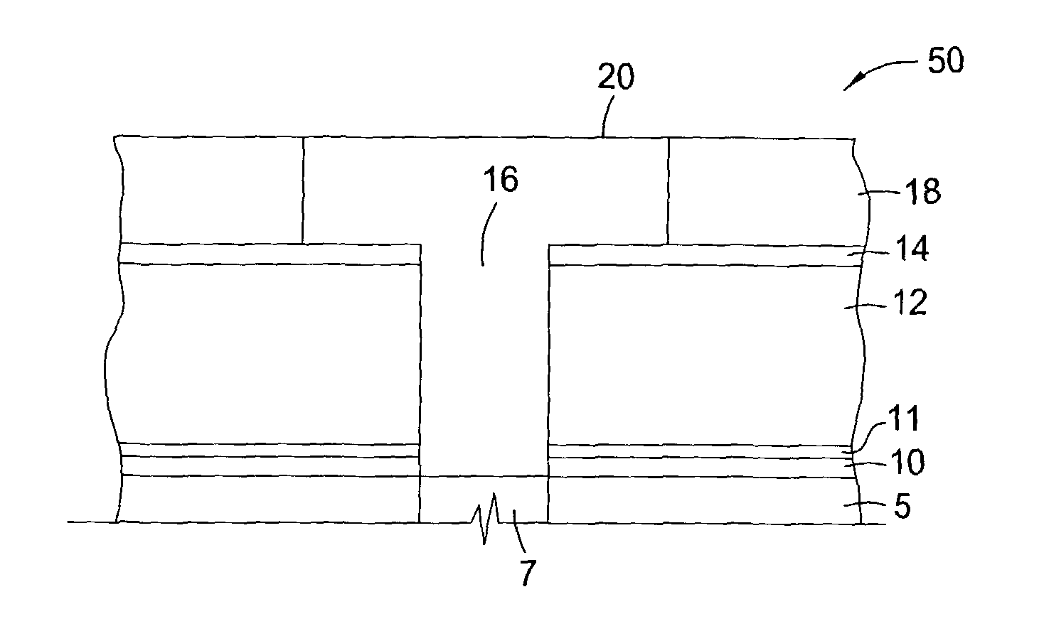
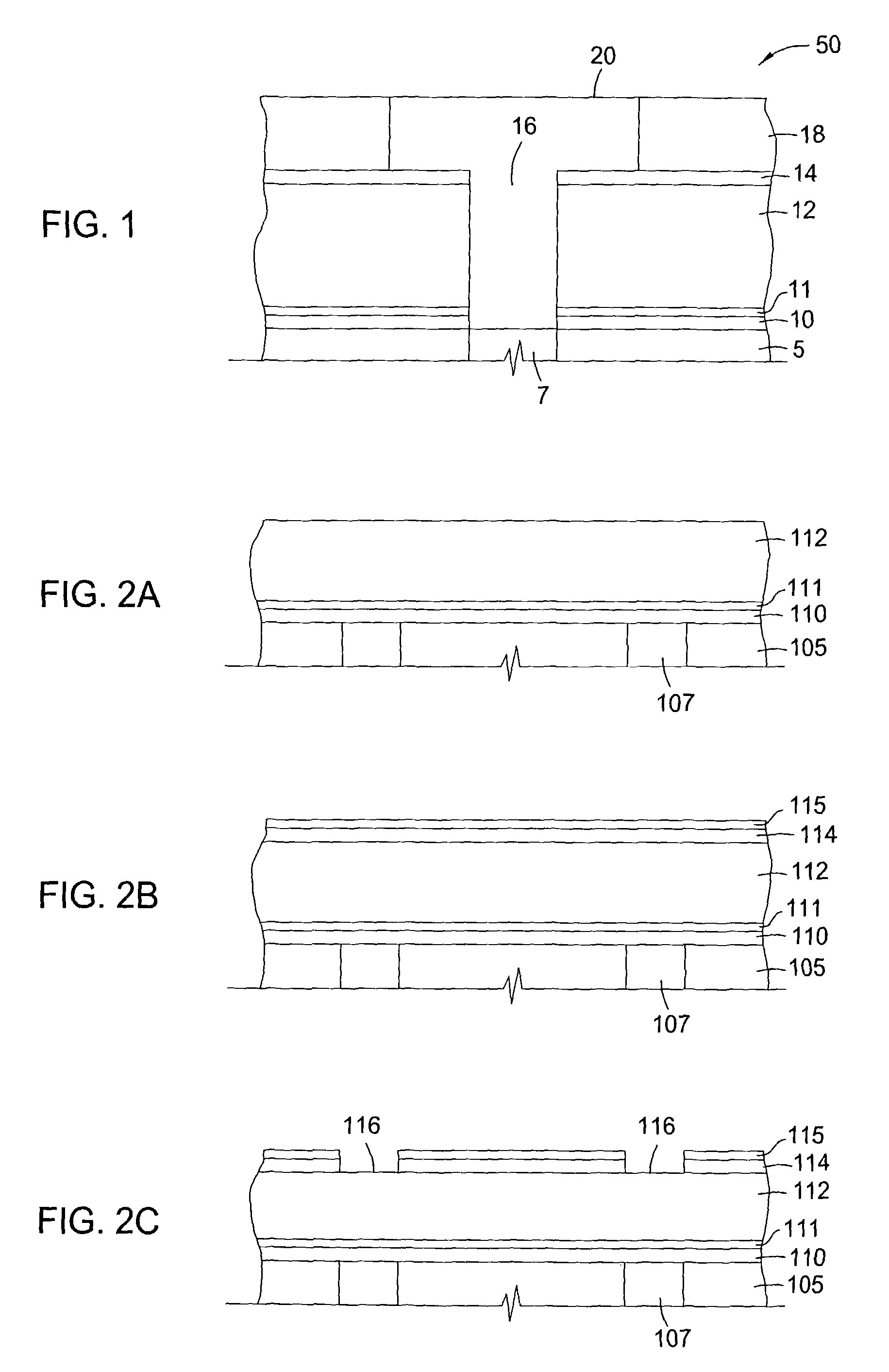
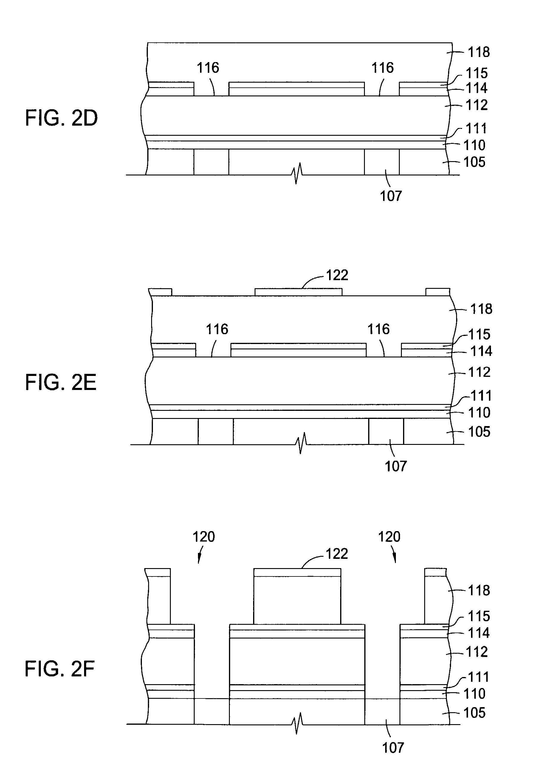
[0066]Organosilicon compounds described herein were deposited as barrier layers on a substrate surface and analyzed. In one example, a silicon carbide barrier film was deposited from a diphenylsilane compound and compared to a silicon carbide barrier film from a conventional silicon carbide precursor, trimethylsilane.

[0067]Both diphenylsilane and trimethylsilane precursors were deposited by introducing diphenylsilane or trimethylsilane at about 500 mg / min into the processing chamber, introducing helium at about 500 sccm into the processing chamber, generating a plasma in the processing chamber by applying 100 watts of RF energy, maintaining the substrate temperature at about 290° C., maintaining the chamber pressure at about 3 Torr to deposit a silicon carbide layer. The heater spacing was about 450 mils from the substrate surface.

[0068]The deposited films were examined and analyzed for dielectric constant and barrier layer diffusion. The diphenylsilane silicon carbide film had a me...


PUM

PropertyMeasurementUnit
dielectric constantaaaaaaaaaa
feature sizesaaaaaaaaaa

Abstract

A method is provided for processing a substrate including providing a processing gas comprising an organosilicon compound comprising a phenyl group to the processing chamber, and reacting the processing gas to deposit a low k silicon carbide barrier layer useful as a barrier layer in damascene or dual damascene applications with low k dielectric materials. A method is provided for depositing a silicon carbide cap layer that has substantially no phenyl groups attached to silicon atoms from a processing gas comprising an oxygen-free organosilicon compound on a low k silicon carbide barrier layer.

Description

BACKGROUND OF THE INVENTION[0001]1. Field of the Invention[0002]The invention relates to the fabrication of integrated circuits, more specifically to a process for depositing dielectric layers on a substrate, and to the structures formed by the dielectric layer. The invention further relates to a process for depositing barrier layers on a substrate, and to the structures formed by the barrier layers.[0003]2. Description of the Related Art[0004]Semiconductor device geometries have dramatically decreased in size since such devices were first introduced several decades ago. Since then, integrated circuits have generally followed the two year / half-size rule (often called Moore's Law), which means that the number of devices that will fit on a chip doubles every two years. Today's fabrication plants are routinely producing devices having 0.35 μm and even 0.18 μm feature sizes, and tomorrow's plants soon will be producing devices having even smaller geometries.[0005]To further reduce the s...

Claims


Application Information

Patent Timeline
06 Jul 2010
Publication
US7749563B2
IPC
C23C16/00; C23C16/02; C23C16/32; H01L21/314; H01L21/768
CPC
C23C16/0272; C23C16/325; H01L21/314; H01L21/7681; H01L21/76826; H01L21/76832; H01L21/02274; H01L21/02167
Inventors
ZHENG, YI; NEMANI, SRINIVAS D.