

Method to form upward pointing p-i-n diodes having large and uniform current
a technology of upward pointing pins and diodes, which is applied in the direction of transistors, digital storage, instruments, etc., can solve the problem of difficulty in forming a large population of vertically oriented p-i-n diodes
- Summary
- Abstract
- Description
- Claims
- Application Information
AI Technical Summary
Benefits of technology
Problems solved by technology
Method used
Image

Examples
example
[0036]Turning to FIG. 7a, formation of the memory begins with a substrate 100. This substrate 100 can be any semiconducting substrate known in the art, such as monocrystalline silicon, IV-IV compounds like silicon-germanium or silicon-germanium-carbon, III-V compounds, II-VII compounds, epitaxial layers over such substrates, or any other semiconducting material. The substrate may include integrated circuits fabricated therein.
[0037]An insulating layer 102 is formed over substrate 100. The insulating layer 102 can be silicon oxide, silicon nitride, Si—C—O—H film, or any other suitable insulating material.
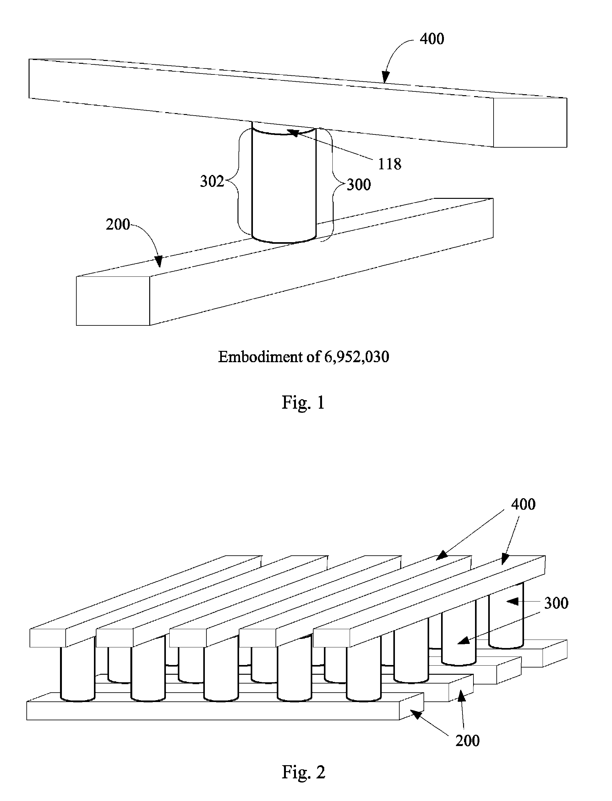
[0038]The first conductors 200 are formed over the substrate 100 and insulator 102. An adhesion layer 104 may be included between the insulating layer 102 and the conducting layer 106 to help conducting layer 106 adhere to insulating layer 102. If the overlying conducting layer 106 is tungsten, titanium nitride is preferred as adhesion layer 104. Conducting layer 106 can comprise any...
PUM
 Abstract
Description
Claims
Application Information