Electronic circuit

a technology of electronic circuits and circuits, applied in the direction of high-frequency circuit adaptations, electrical apparatus construction details, inductances, etc., can solve the problems of communication bandwidth, system cost, and lowering of yield, so as to increase the sn ratio, reduce the cost of system maintenance, and efficiently transmit signals

Active Publication Date: 2010-08-03
THRUCHIP JAPAN INC
View PDF9 Cites 32 Cited by
  • Summary
  • Abstract
  • Description
  • Claims
  • Application Information

AI Technical Summary

Benefits of technology

[0015]In addition, because the first substrate also includes a transmitter circuit for outputting signals to the first coil when transmission digital data changes, power consumption can be reduced.
[0018]Still further, because the second substrate also includes a receiver circuit that receives signals only for a predetermined cyclic period, it is possible to increase the SN ratio.
[0019]According to the present invention, it is possible to efficiently transmit signals where signals are transmitted over substrates with three or more substrates three-dimensionally mounted.
[0020]Also, because communications are carried out by current drive, the electronic circuit according to the present invention can be favorably employed for LSIs, and the like in which low voltage drive is highly demanded.

Problems solved by technology

This system is made expensive because different process technologies are realized on one bare chip, and the yield thereof is lowered due to an increase in the chip area.
In this case, the number of connections between chips is the same as in a conventional package or less, wherein a problem occurs in the communications bandwidth.
In addition, three-dimensional mounting is indispensable when reducing the mounting area, wherein since, in the wire bonding system, it is necessary to make chips smaller that are to be stacked up, it is difficult to form a bus because the mounting area is restricted and major connections are based on one-to-one connection.
However, as regards mounting of three or more chips, it is necessary to physically produce a communications path passing through a chip itself or a build-up substrate, a so-called “through hole,” wherein an exclusive process technology and highly precise processing accuracy are demanded: resulting in an increase in production costs.
Although, for face-to-face mounting up to two chips, costs thereof are inexpensive and high-speed communications are possible, transmission efficiency of signals is radically worsened in three or more chips, wherein power consumption is increased.
However, even in the case of using an antenna, where signals are attempted to be transmitted over chips with three or more chips mounted, it is necessary that an electric field generated by the antenna passes through a number of substances whose dielectric constants are different from each other (biased silicon substrate, doped silicon, oxide film, nitride film, etc.), wherein reflection is generated at a boundary phase, resulting in a worsening in transmission efficiency.

Method used


Image

  • Electronic circuit
  • Electronic circuit
  • Electronic circuit

Examples


Embodiment Construction

[0049]Hereinafter, a detailed description is given of preferred embodiments of the present invention with reference to the accompanying drawings.

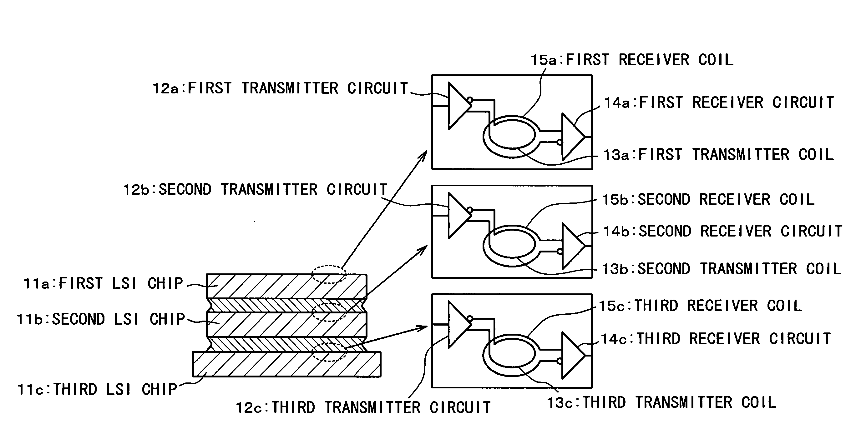
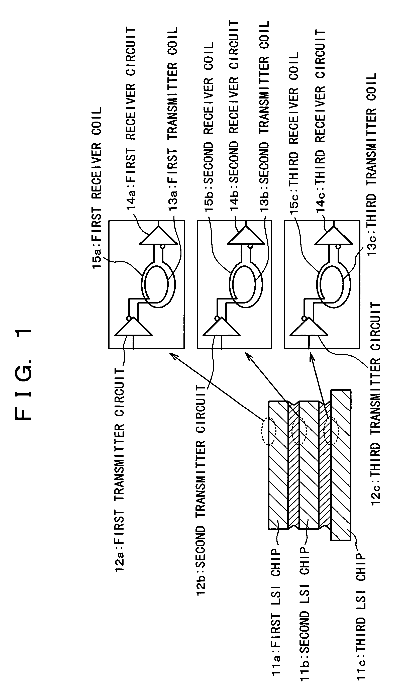
[0050]FIG. 1 is a view depicting a configuration of an electronic circuit according to one embodiment of the present invention. The electronic circuit according to the present embodiment is composed of a first LSI chip 11a, a second LSI chip 11b and a third LSI chip 11c. This is an example in which LSI chips are stacked up in three layers and a bus is formed so as to lie across three chips. The first through the third LSI chips 11a, 11b and 11c are vertically stacked up, and the respective chips are fixed to each other with an adhesive agent. The first through the third transmitter coils 13a, 13b and 13c, which are respectively used for transmission, are formed by wiring on the first through the third LSI chips 11a, 11b and 11c, and also, the first through the third receiver coils 15a, 15b and 15c, which are respectively used for receiving,...


PUM

PropertyMeasurementUnit
voltageaaaaaaaaaa
transmission efficiencyaaaaaaaaaa
dielectric constantsaaaaaaaaaa

Abstract

An electronic circuit capable of efficiently transmitting signals in a case where signals are transmitted over substrates with three or more substrates three-dimensionally mounted. In the present invention, LSI chips are stacked in three layers, and a bus is formed over three chips. The first through the third transmitter coils 13a, 13b, 13c and the first through the third receiver coils 15a, 15b, 15c are formed by wiring on the first through the third LSI chips 11a, 11b, 11c. These three pairs of transmitter and receiver coils are disposed so that the centers of the openings thereof are coincident with each other, whereby three pairs of transmitter and receiver coils 13 and 15 form inductive coupling to enable communications. The first through the third transmitter circuits 12a, 12b, 12c are connected to the first through the third transmitter coils 13a, 13b and 13c, respectively, and the first through the third receiver circuits 14a, 14b, 14c are connected to the first through the third receiver coils 15a, 15b, 15c, respectively.

Description

BACKGROUND OF THE INVENTION[0001]1. Field of the Invention[0002]The present invention relates to an electronic circuit that is capable of suitably carrying out communications between substrates such as IC (Integrated Circuit) bare chips, and PCBs (Printed Circuit Boards).[0003]2. Description of the Related Art[0004]Downsizing and high performance have been further advanced in recent electronic devices. In line therewith, incorporated LSIs (Large Scale Integration) have been downsized and high speed processing has progressed. As means for achieving downsizing and high-speed processing, it is desirable that entire functions are included in one package, and now generally two types of realization methods exist.[0005]As the first method, a system called “system on chip (SoC)” is available, which incorporates the entire system on a single bare chip. This system is made expensive because different process technologies are realized on one bare chip, and the yield thereof is lowered due to a...

Claims


Application Information

Patent Timeline
Patent Type & Authority Patents(United States)
IPC IPC(8): H05K7/00H01L25/00H01L25/065H01L25/07H01L25/18H05K1/02H05K1/16
CPCH01L25/0657H05K1/165H01F17/0006H01F2038/143H01L2225/06527Y10T29/49002H05K1/0239H01L2224/32145H05K1/0237H01L25/00H01L25/04
Inventor KURODA, TADAHIROMIZOGUCHI, DAISUKEYUSOF, YUSMEERAZ BINTIMIURA, NORIYUKISAKURAI, TAKAYASU
Owner THRUCHIP JAPAN INC
Why Eureka
Try Eureka