Method of catastrophic transfer of a thin film after co-implantation

a technology of co-implantation and thin film, which is applied in the direction of basic electric elements, semiconductor/solid-state device manufacturing, electric devices, etc., can solve the problems of affecting the crystalline reducing the quality of the material, and reducing the possibility of crystalline defects during the following treatment, so as to achieve high mechanical stress, low roughness of the surface, and high quality

Active Publication Date: 2010-08-10
COMMISSARIAT A LENERGIE ATOMIQUE ET AUX ENERGIES ALTERNATIVES +1
View PDF114 Cites 21 Cited by
  • Summary
  • Abstract
  • Description
  • Claims
  • Application Information

AI Technical Summary

Benefits of technology

[0014]The present invention relates to a method of transferring a thin layer leading to low roughness of the surface of the transferred layer, and not involving high mechanical stresses in case of materials having high differences in expansion coefficients. In other words, the object of the invention is to obtain, for a moderate cost, thin films of high quality, thereby avoiding at the same time the drawbacks of a heat treatment at high temperature and those related to the utilization of a tool for assisted splitting, and those related to an additional treatment for reducing roughness after splitting.
[0017]So defined, the invention is based on the implantation of two different species. One of the implanted species localizes, depending on its implantation energy, the zone in which splitting will later occur by the formation of specific defects, the other corresponds to a type of atoms trapped in that zone which will promote the extension of the specific defects designated previously, apparently: by increasing the weakening of the implanted zone at relatively low temperature by preventing, in the case of the implantation of a silicon substrate by hydrogen, the Si—H dissociation (thereby promoting the H-defects of platelet type) and putting those defects under pressure.
[0022]2) there is no longer assisted splitting since the catastrophic fracture enables the fracture wave to be propagated instantaneously and without fits and starts over the entire section of the wafer; it is not necessary for any blade whatsoever to penetrate between the substrate and the future thin film, which considerably improves the topology of the surfaces thus freed (thus with lower roughness), and avoids crown defects, which makes the entire thin film usable, including its periphery; the fact of no longer having to introduce a tool is also favorable to the industrialization of the method.
[0023]Given that, at latest at the moment of the heat treatment, the source substrate is placed in intimate contact by said face with a stiffener or target substrate, the heat treatment contributes to improving the bonding energy between those substrates.
[0027]In fact, tests with a co-implantation of hydrogen and helium in the source substrate in the conditions of the invention have lead to catastrophic splitting, that is to say to complete and virtually instantaneous splitting, with a continuous and planar propagation of the fracture wave, initiated with the help of a very low localized provision of energy, which in particular had the advantage of avoiding surface undulations, that is to say avoiding large variations in surface roughness after fracture, in comparison with progressive splitting. Due to this, that catastrophic splitting implies less polishing afterwards.
[0032]The radical difference in this method, with respect to the technique described by above-referenced article by Henttinen et al., is that it is not necessary to carry out excess dosage of the hydrogen which can greatly damage the implanted zone. The effect of the co-implantation makes it possible to achieve the maximum weakening of that zone at the temperature sufficient for solidity of the bonding interfaces without involving additional processes (plasma chemical activation and RCA1). Furthermore, the invention leads to reduced roughness of the transferred film in comparison with that obtained by thermal splitting.

Problems solved by technology

These defects may be micro-bubbles and / or platelets and / or micro-cavities and / or dislocation loops and / or other crystalline defects, locally disrupting the crystalline quality of the material; their nature, density and size are strongly dependent on the species implanted (typically hydrogen) as well as on the nature of the source substrate.
This renders the treatment steps that follow more difficult.
For example, the transferred film must be polished more and there is a risk of crystalline defects being created during the following treatments.
Furthermore, in heterostructures (comprising a superposition of substrates of different materials), another technological problem encountered is the presence of a field of very high stresses in the various films in contact, during the heat treatment, due to the difference in the coefficients of thermal expansivity of the various materials placed in contact.
This may induce the degradation of the heterostructures if the thermal splitting occurs at a temperature higher than a critical temperature.
For example, an excess dose of the implanted species may increase the weakening of the implanted zone in which the splitting at low temperature occurs.
This approach, although reducing the roughness of the transferred surface by of the order of half with respect to conventional splitting solutions that are purely thermal and without plasma activation, involves a step of plasma chemical activation followed by wet chemical cleaning known to those skilled in the art as RCA1 cleaning, which may represent a significant drawback from an industrial point of view, such as increased cost.
Thus, it has been found that, if the thermal budget is too low, the transfer of the thin film is of poor quality, whereas if it is too high, fracture may occur of one of the substrates in the case of a heterostructure.
The narrow operational parameters, however, constitute a heavy constraint for industrial exploitation.
This type of fracture leads to the following defects, at the future surface freed by the splitting of the thin film: 1) crown defect (non-transferred zone, at the periphery of the final product), for example related to a local bonding energy too low with respect to the rest of the interface, and to the introduction of tools to start off the transfer; 2) lack of uniformity (low frequency roughness) of the thickness of the thin film transferred, in particular due to the fracture wave assisted mechanically, thus irregular, by fits and starts, which then necessitates treatments, such as polishing, which it is however generally sought to avoid, 3) difficult industrial implementation, given the use of a tool which accompanies the propagation of the fracture, which implies an individual treatment of each structure (or wafer).
However, Cerofolini et al. do not deduce practical conclusions therefrom as to the manner of obtaining thin films of good quality (in particular in relation to the state of the surface) for a moderate cost.

Method used


Image

  • Method of catastrophic transfer of a thin film after co-implantation
  • Method of catastrophic transfer of a thin film after co-implantation

Examples


examples

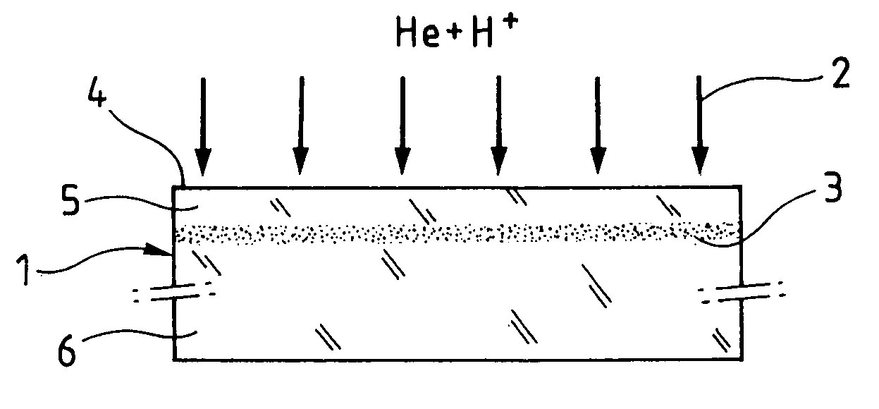
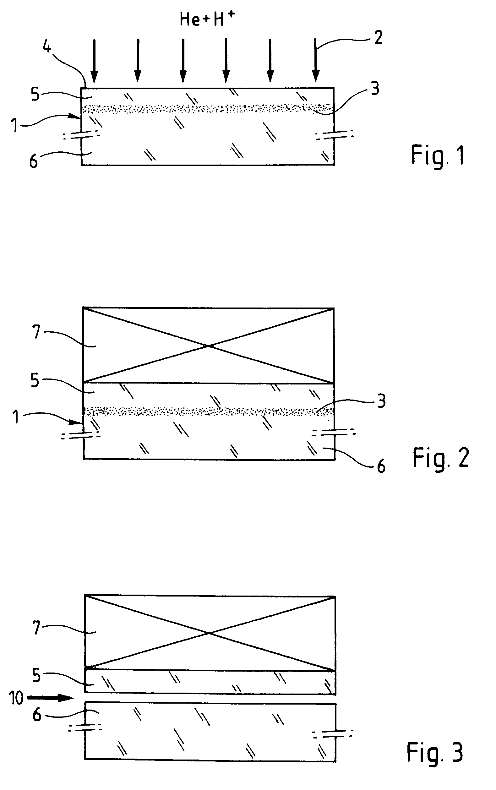
[0066]According to a first embodiment of the invention, a substrate of Si (˜700 μm) comprising a layer of thermal SiO2 on the surface (for example 145 nm) was implanted initially with helium atoms under implantation conditions of 70 keV at 1×10¹⁶ ions / cm2, and then implanted with hydrogen atoms under implantation conditions of 30 keV at 4.25×10¹⁶ ion s / cm2. This source substrate was next joined to a target substrate of Si (˜700 μm) by direct bonding. A heat treatment around 350° C. induced the growth of cavities of platelet type localized at the hydrogen concentration peak. The helium atoms play the role of atoms trapped thereat and create a maximum of defects of platelet type at the applied temperature. After a certain time (for example 2 hours), with scarcely the commencement of insertion of a blade between the bonding interfaces in the form of a shock, catastrophic splitting at the location of maximum hydrogen concentration led to the transfer of the thin film of Si onto the targ...


PUM


Abstract

The invention relates to a method of catastrophic transfer of a thin film including implanting in a source substrate a first species of ions or gas at a given depth and a second species of ions or gas, the first species being adapted to generate defects and the second species being adapted to occupy those defects. The process further includes applying a stiffener in intimate contact with the source substrate, applying a heat treatment to that source substrate, at a given temperature for a given time, so as to create, substantially at the given depth, a buried weakened zone, without initiating the thermal splitting of a thin film, and applying a localized amount of energy, for example mechanical stresses, to that source substrate so as to provoke the catastrophic splitting of a thin film, the thin film having a substantially planar face opposite to the face surface of the source substrate.

Description

RELATED APPLICATIONS[0001]This application claims priority to U.S. provisional patent application Ser. No. 60 / 531,591, filed Dec. 19, 2003.FIELD OF THE INVENTION[0002]The invention relates, generally, to methods for forming a thin-film in a semiconductor substrate and, more particularly, to a method of transferring an ultra-thin film (the term thin film is also used) at low temperature by the method of co-implantation. The invention has applications in particular in the fields of micro-electronics, micro-mechanics, optics and integrated electronics.BACKGROUND[0003]As is known, splitting a thin film may be achieved by implantation of chemical species in a source substrate, for example of silica, to induce the formation of a zone of defects at a particular depth. These defects may be micro-bubbles and / or platelets and / or micro-cavities and / or dislocation loops and / or other crystalline defects, locally disrupting the crystalline quality of the material; their nature, density and size a...

Claims


Application Information

Patent Timeline
Patent Type & Authority Patents(United States)
IPC IPC(8): H01L21/30H01L21/46H01L21/762
CPCH01L21/76254
Inventor NGUYEN, NGUYET-PHUONGCAYREFOURCQ, IANLAGAHE-BLANCHARD, CHRISTELLE
Owner COMMISSARIAT A LENERGIE ATOMIQUE ET AUX ENERGIES ALTERNATIVES
Why Eureka
Try Eureka