Semiconductor integrated circuit device and delay fault testing method

a technology of integrated circuit device and delay fault, which is applied in the direction of testing circuit, resistance/reactance/impedence, instruments, etc., can solve the problems of individual study not practicable, error in delay fault test, and complex manufacture defects

Inactive Publication Date: 2010-08-17
RENESAS ELECTRONICS CORP
View PDF16 Cites 7 Cited by
  • Summary
  • Abstract
  • Description
  • Claims
  • Application Information

AI Technical Summary

Benefits of technology

[0032]Also, a signal route from an output of the first flip-flop to an input of the second flip-flop may be a timing exception path which is not necessary for a delay time to fall within a one clock cycle of the clock signal.
[0041]According to the present invention, it is possible to provide the delay fault testing circuit for testing the delay fault without any drop in the delay fault detection rate and the method of testing the same.

Problems solved by technology

In recent years, a larger scale and higher speed of a system LSI (Large Scale Integrated Circuit) has been advanced, and in association with the miniaturization of an LSI manufacturing process to support this advancement, a manufacture defect becomes more complex, which reveals an operational error of the LSI caused due to a delay fault.
In the path delay fault, it is assumed that a delay time along one path is delayed, so that a fault is caused due to a path route itself.
When a delay from a period td of the clock cycle C11 is present, the flip-flop 17 cannot latch the change in the output of the NOR circuit 34, and this results in an error in the delay fault test.
However, in the test pattern of the large LSI, the individual study is not practical.
Therefore, the delay fault detection of the usual path route where the timing exception path and the final flip-flop are same cannot be performed, which reduces a delay fault detection rate of the transition delay fault model.
Thus, the delay fault cannot be detected.
However, the conventional delay fault testing circuit could not attain this.

Method used


Image

  • Semiconductor integrated circuit device and delay fault testing method
  • Semiconductor integrated circuit device and delay fault testing method
  • Semiconductor integrated circuit device and delay fault testing method

Examples


first embodiment

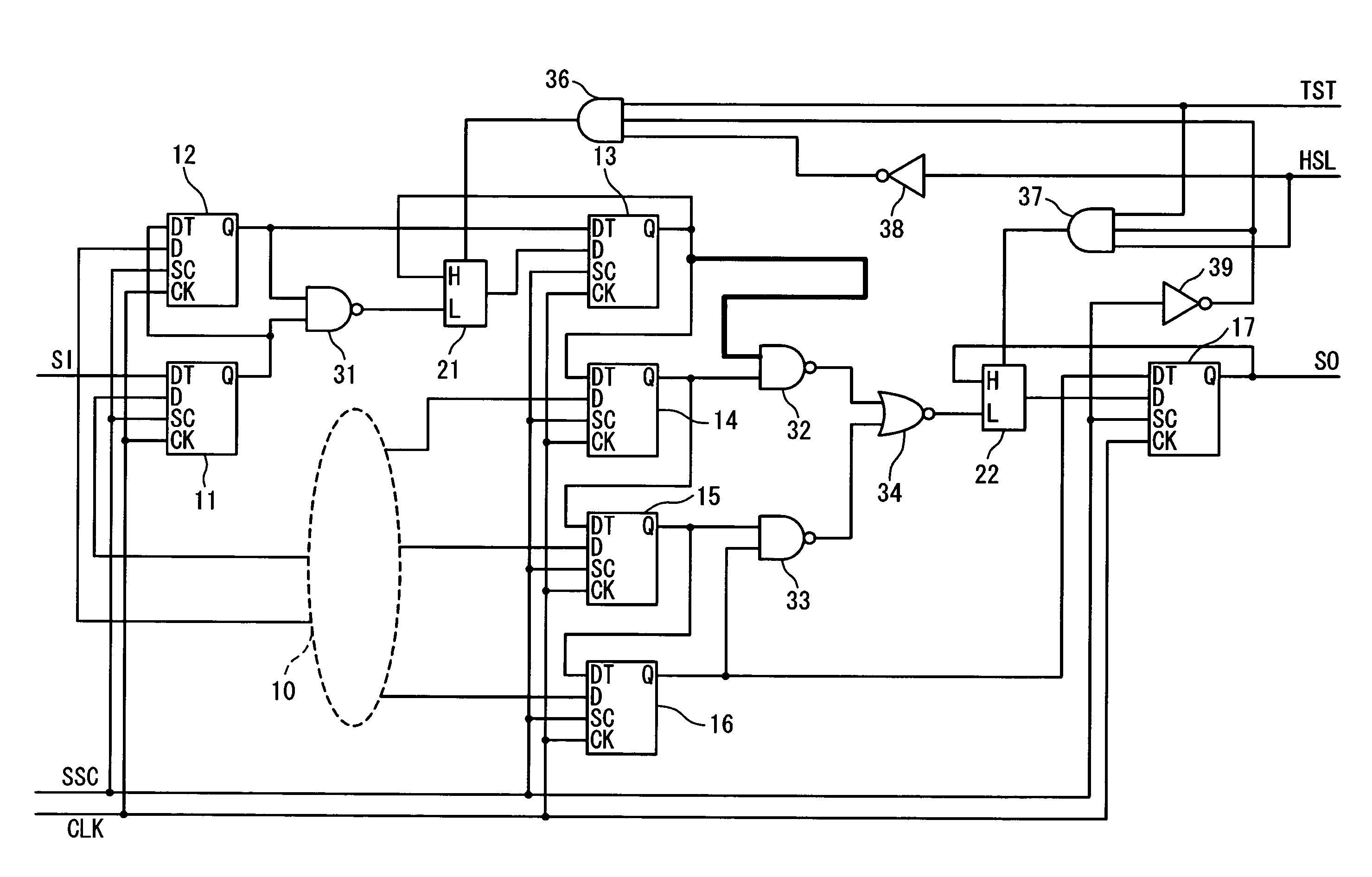
[0056]FIG. 6 shows the semiconductor integrated circuit device including a delay fault testing circuit according to the first embodiment of the present invention. Referring to FIG. 6, the delay fault testing circuit contains flip-flops 11 to 17 with a scan path test function, a combination circuit 10, selecting circuits 21 and 22, NAND circuits 31 to 33, a NOR circuit 34, AND circuits 36 and 37 and inverter circuits 38 and 39. Each of the flip-flops 11 to 17 does not have a data holding function, as shown in FIGS. 13A to 13C. Hereinafter, the flip-flops 11 to 17 with the scan path test function are simply referred to as the flip-flops 11 to 17.

[0057]In each of the flip-flops 11 to 17, a clock signal CLK is sent to a clock terminal CK, and a scan shift control signal SSC is sent to a scan shift control terminal SC. At the time of the scan path test, the flip-flops 11 to 17 form a scan path, and an output terminal Q of a former flip-flop is connected to a scan-in terminal DT of a curr...

second embodiment

[0078]FIG. 10 shows the semiconductor integrated circuit device of a delay fault testing circuit according to the second embodiment of the present invention. In this delay fault testing circuit, the hold control signal HSL is generated by the flip-flop 18. Then, the output of the flip-flop 18 is set as the test data through the scan path externally. Thus, in the delay fault testing circuit shown in FIG. 10, the flip-flop 18 is added to the delay fault testing circuit shown in FIG. 6, and its output signal is sent as the hold control signal HSL to each section. The scan-in terminal DT of the flip-flop 18 is connected to the output terminal Q of the flip-flop 17, and the data input terminal D is connected to its own output terminal Q. The clock signal CLK is sent to the clock terminal CK, and the scan shift control signal SSC is sent to the scan shift control terminal SC. Therefore, the flip-flop 18 is connected to be added to the final portion of the scan path composed of the flip-fl...


PUM


Abstract

A semiconductor integrated circuit device includes a plurality of flip-flops configured to form a scan chain in a scan path test to operate as a shift register. The first flip-flop of the plurality of flip-flops latches a first input signal in synchronization with a clock signal, outputs a first output signal and fixes the first output signal based on the first selection control signal. A second flip-flop of the plurality of flip-flops latches a second input signal in synchronization with the clock signal, outputs a second output signal, and fixes the second output signal based on a second selection control signal. The semiconductor integrated circuit device further includes a control circuit configured to generate the first and second selection control signals such that a period during which the first flip-flop fixes the first output signal is different from a period during which the second flip-flop fixes the second output signal.

Description

BACKGROUND OF THE INVENTION[0001]1. Field of the Invention[0002]The present invention relates to a semiconductor integrated circuit device, and more particularly relates to a scan path testing circuit built in a semiconductor integrated circuit device, and a delay fault testing method that uses the scan path testing circuit.[0003]2. Description of the Related Art[0004]In recent years, a larger scale and higher speed of a system LSI (Large Scale Integrated Circuit) has been advanced, and in association with the miniaturization of an LSI manufacturing process to support this advancement, a manufacture defect becomes more complex, which reveals an operational error of the LSI caused due to a delay fault. For this reason, the importance of a delay fault test in the system LSI becomes higher. As a method of attaining a circuit for the delay fault test, there are several methods, and the delay fault test that uses a scan path testing circuit is widely used.[0005]As a fault model of a dela...

Claims


Application Information

Patent Timeline
Patent Type & Authority Patents(United States)
IPC IPC(8): G01R31/28
CPCG01R31/318536
Inventor FURUYA, NOBUO
Owner RENESAS ELECTRONICS CORP
Why Eureka
Try Eureka