Process using combined capacitively and inductively coupled plasma sources for controlling plasma ion radial distribution

a plasma source and capacitive coupled technology, applied in the direction of fluid pressure measurement, instruments, vacuum gauges, etc., can solve the problems of not all process parameters can be independently controlled, non-uniform plasma density is introduced into the processing, and non-uniformity becomes more critical, so as to increase the reaction rate and etch rate, increase the dissociation in the plasma, and increase the ion density

Inactive Publication Date: 2010-08-24
APPLIED MATERIALS INC
View PDF110 Cites 20 Cited by
  • Summary
  • Abstract
  • Description
  • Claims
  • Application Information

AI Technical Summary

Problems solved by technology

In semiconductor fabrication processes, conventional sources of plasma source power, such as inductively coupled RF power applicators or capacitively couple RF power applicators, introduce inherent plasma density non-uniformities into the processing.
As device geometries have continued to shrink, such non-uniformities become more critical, requiring better compensation.
However, a large ceiling-to-wafer distance can prevent the beneficial gas distribution effects of a ceiling gas distribution showerhead from reaching the wafer surface, due to diffusion over the large distance.
One limitation of such reactors is that not all process parameters can be independently controlled.
But, this increases the dissociation in the plasma, which can reduce etch selectivity and increase etch microloading problems, in some cases.
Thus, the etch rate must be limited to those cases where etch selectivity or microloading are critical.
Another problem arises in the processing (e.g., etching) of multi-layer structures having different layers of different materials.
However, to idealize the processing conditions for each sub-layer of the structure being etched would require different process reactors, and this is not practical.

Method used


Image

  • Process using combined capacitively and inductively coupled plasma sources for controlling plasma ion radial distribution
  • Process using combined capacitively and inductively coupled plasma sources for controlling plasma ion radial distribution
  • Process using combined capacitively and inductively coupled plasma sources for controlling plasma ion radial distribution

Examples


Embodiment Construction

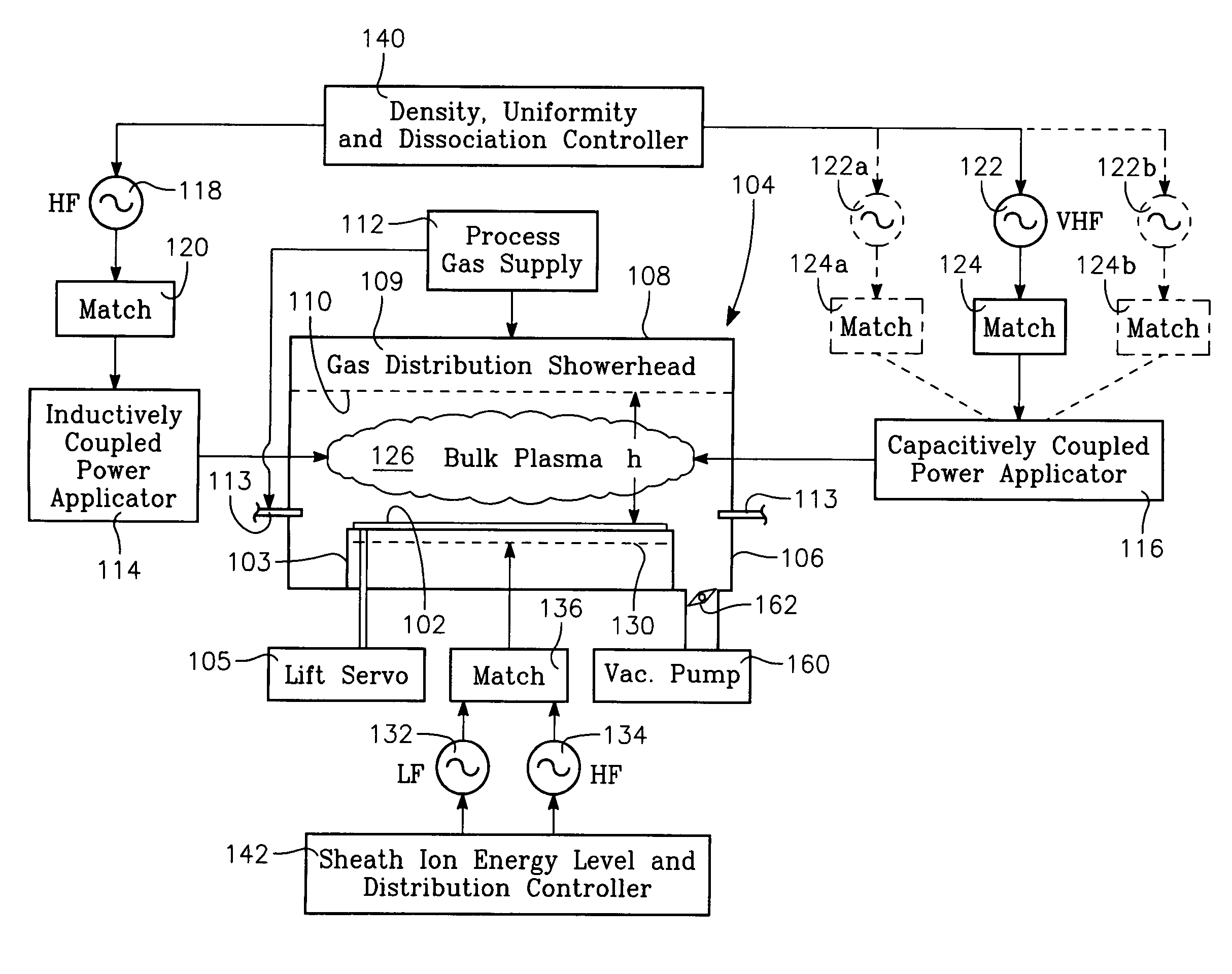
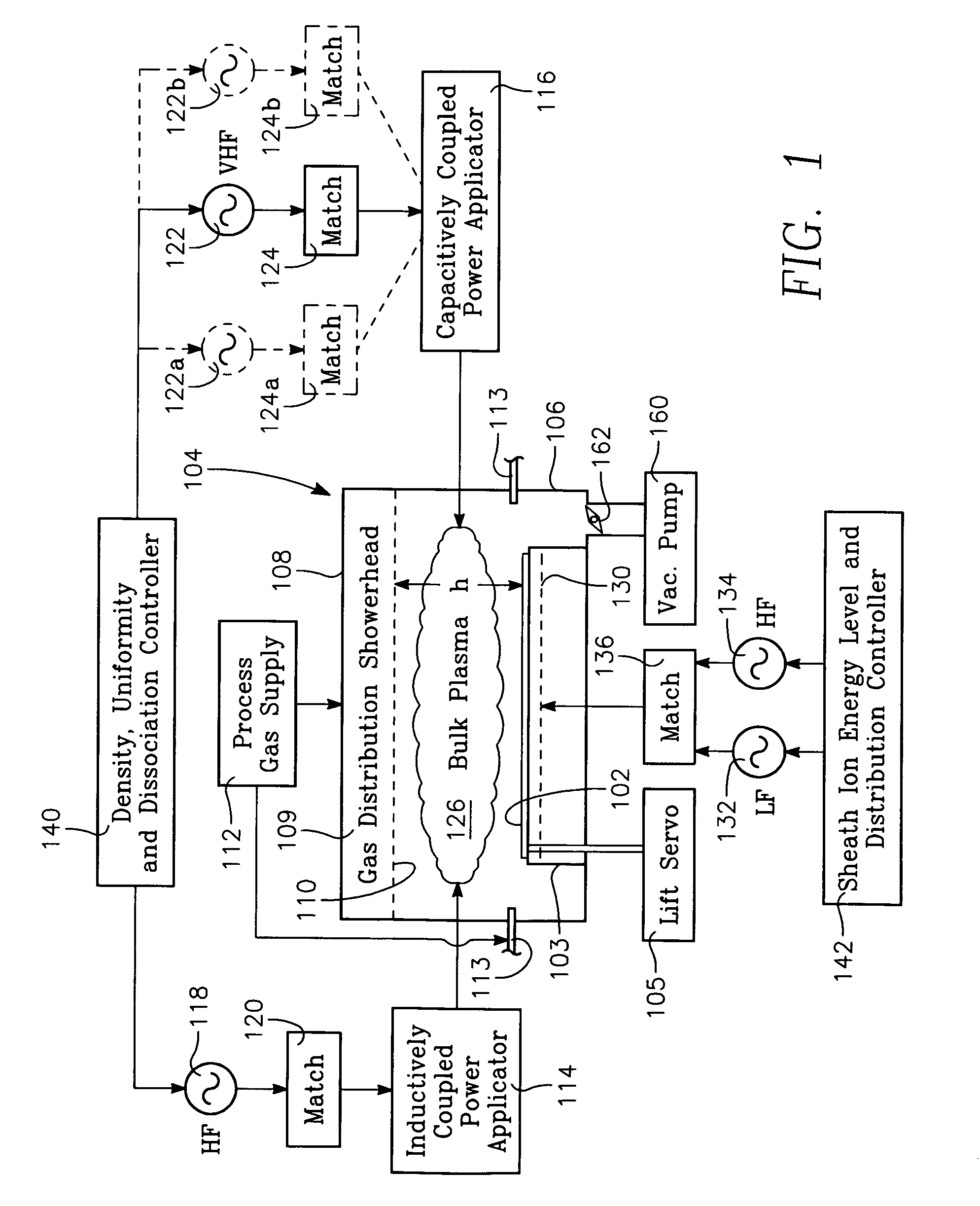
[0026]FIG. 1 depicts a plasma reactor for processing a workpiece 102, which may be a semiconductor wafer, held on a workpiece support 103, which may (optionally) be raised and lowered by a lift servo 105. The reactor consists of a chamber 104 bounded by a chamber sidewall 106 and a ceiling 108. The ceiling 108 may comprise a gas distribution showerhead 109 having small gas injection orifices 110 in its interior surface, the showerhead 109 receiving process gas from a process gas supply 112. In addition, process gas may be introduced through gas injection nozzles 113. The reactor includes both an inductively coupled RF plasma source power applicator 114 and a capacitively coupled RF plasma source power applicator 116. The inductively coupled RF plasma source power applicator 114 may be an inductive antenna or coil overlying the ceiling 108. In order to permit inductive coupling into the chamber 104, the gas distribution showerhead 109 may be formed of a dielectric material such as a ...


PUM

PropertyMeasurementUnit
frequencyaaaaaaaaaa
frequencyaaaaaaaaaa
frequencyaaaaaaaaaa

Abstract

A method of processing a workpiece in the chamber of a plasma reactor in which the plasma ion density radial distribution in the process region is controlled by adjusting the ratio between the amounts of the (VHF) capacitively coupled power and the inductively coupled power while continuing to maintain the level of total plasma source power. The method can also include applying independently adjustable LF bias power and HF bias power to the workpiece and adjusting the average value and population distribution of ion energy at the surface of the workpiece by adjusting the proportion between the LF and HF bias powers.

Description

BACKGROUND OF THE INVENTION[0001]In semiconductor fabrication processes, conventional sources of plasma source power, such as inductively coupled RF power applicators or capacitively couple RF power applicators, introduce inherent plasma density non-uniformities into the processing. In particular, inductively coupled plasma sources are characterized by an “M”-shaped radial distribution of plasma ion density over the semiconductor workpiece or wafer. As device geometries have continued to shrink, such non-uniformities become more critical, requiring better compensation. Presently, the non-uniformity of an overhead inductively coupled source is reduced or eliminated at the wafer surface by optimizing the coil design and ceiling-to-wafer distance, aspect ratio, of the chamber. This distance must be sufficient so that diffusion effects can overcome the effects of the nonuniform ion distribution in the ion generation region before they reach the wafer. For smaller device geometries on th...

Claims


Application Information

Patent Timeline
Patent Type & Authority Patents(United States)
IPC IPC(8): G01L21/30C23F1/00
CPCH01J37/32091H01J37/321H01J37/32165H01J37/32174
Inventor PATERSON, ALEXANDERTODOROW, VALENTIN N.PANAGOPOULOS, THEODOROSHATCHER, BRIAN K.KATZ, DANHAMMOND, IV, EDWARD P.HOLLAND, JOHN P.MATYUSHKIN, ALEXANDER
Owner APPLIED MATERIALS INC
Why Eureka
Try Eureka