Method for manufacturing semiconductor device comprising the step of forming nitride/oxide by high-density plasma

a manufacturing method and semiconductor technology, applied in the direction of semiconductor devices, basic electric elements, electrical appliances, etc., can solve the problem of lowering the reliability of a tft, and achieve the effect of reducing the display defect of the display device and high reliability

Inactive Publication Date: 2010-08-31
SEMICON ENERGY LAB CO LTD
View PDF76 Cites 12 Cited by
  • Summary
  • Abstract
  • Description
  • Claims
  • Application Information

AI Technical Summary

Benefits of technology

[0007]In view of the forgoing problems, it is an object of the present invention to provide a method for manufacturing a semiconductor device, in which reliability of a gate electrode, and a source wiring and a drain wiring is improved, and a highly reliable TFT is intended to be manufactured. Further, it is also an object of the present invention to provide a method for manufacturing a semiconductor device intended to reduce a display defect of a display device.
[0021]A surface of a gate electrode is covered with a dense nitride film by nitriding the surface of the gate electrode by high-density plasma produced in a high-density plasma apparatus, and thus, a heat resistant property of the gate electrode can be improved and the gate electrode can be prevented from being oxidized. Furthermore, since the nitride film formed by high-density plasma produced in the high-density plasma apparatus is a dense film with less plasma damage, reliability of a semiconductor device can be improved.
[0022]A surface of a wiring is covered with a dense nitride film or oxide film by nitriding or oxidizing the surface of the wiring by high-density plasma produced in a high-density plasma apparatus, and thus, a heat resistant property of the wiring can be improved and disconnection of the wiring can be prevented. Furthermore, since the nitride film or the oxide film formed by high-density plasma produced in the high-density plasma apparatus is a dense film with less plasma damage, reliability of a semiconductor device can be improved.
[0023]By nitriding or oxidizing a surface of a pixel electrode by high-density plasma produced in a high-density plasma apparatus, the surface can be reformed without damage due to plasma. Therefore, reliability of a display device can be improved.

Problems solved by technology

However, since the nitride film formed by a CVD method or a sputtering method has a defect inside the film and film quality is not sufficient, there is a concern that reliability of a TFT be lowered.

Method used


Image

  • Method for manufacturing semiconductor device comprising the step of forming nitride/oxide by high-density plasma
  • Method for manufacturing semiconductor device comprising the step of forming nitride/oxide by high-density plasma
  • Method for manufacturing semiconductor device comprising the step of forming nitride/oxide by high-density plasma

Examples


embodiment mode 1

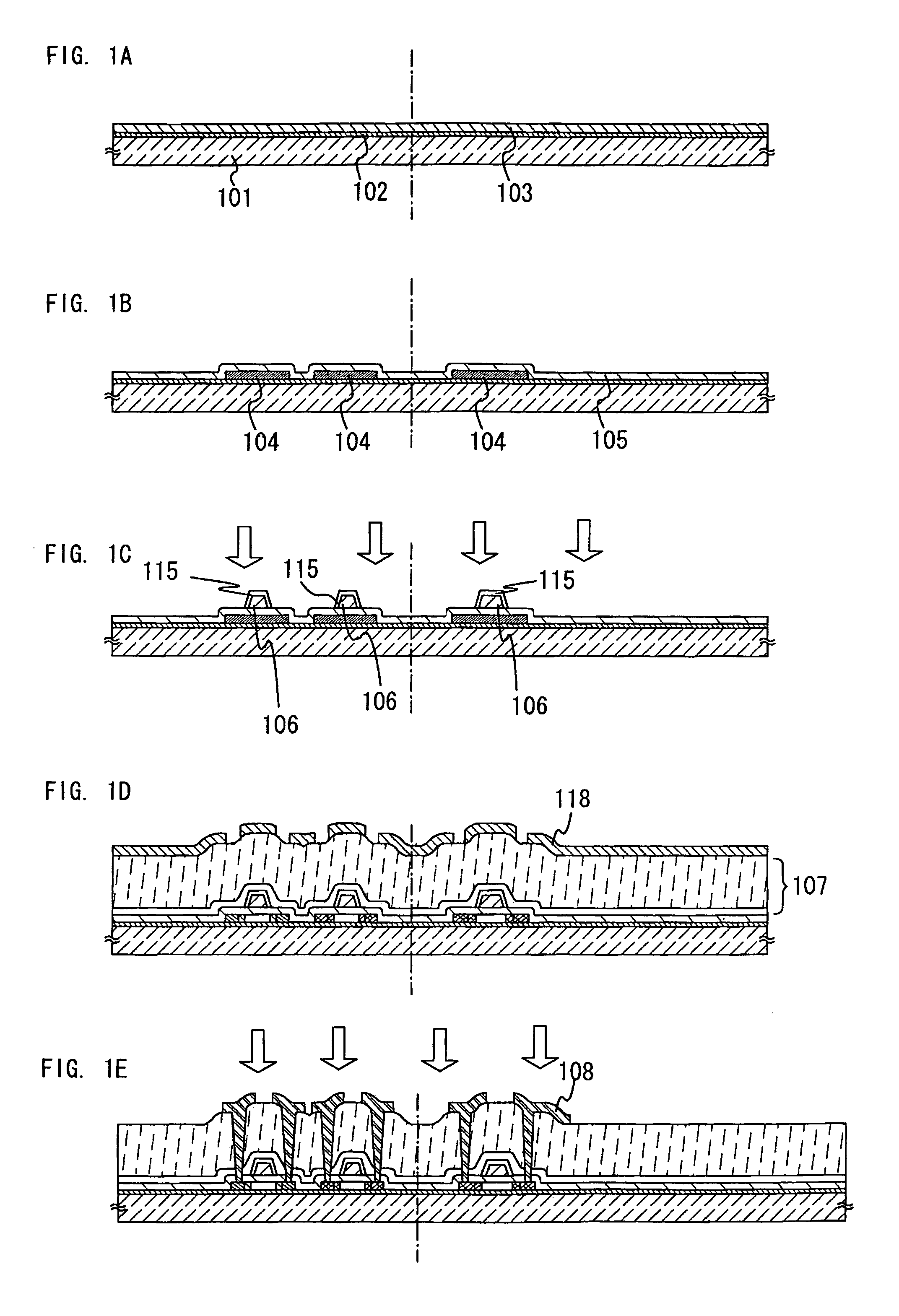
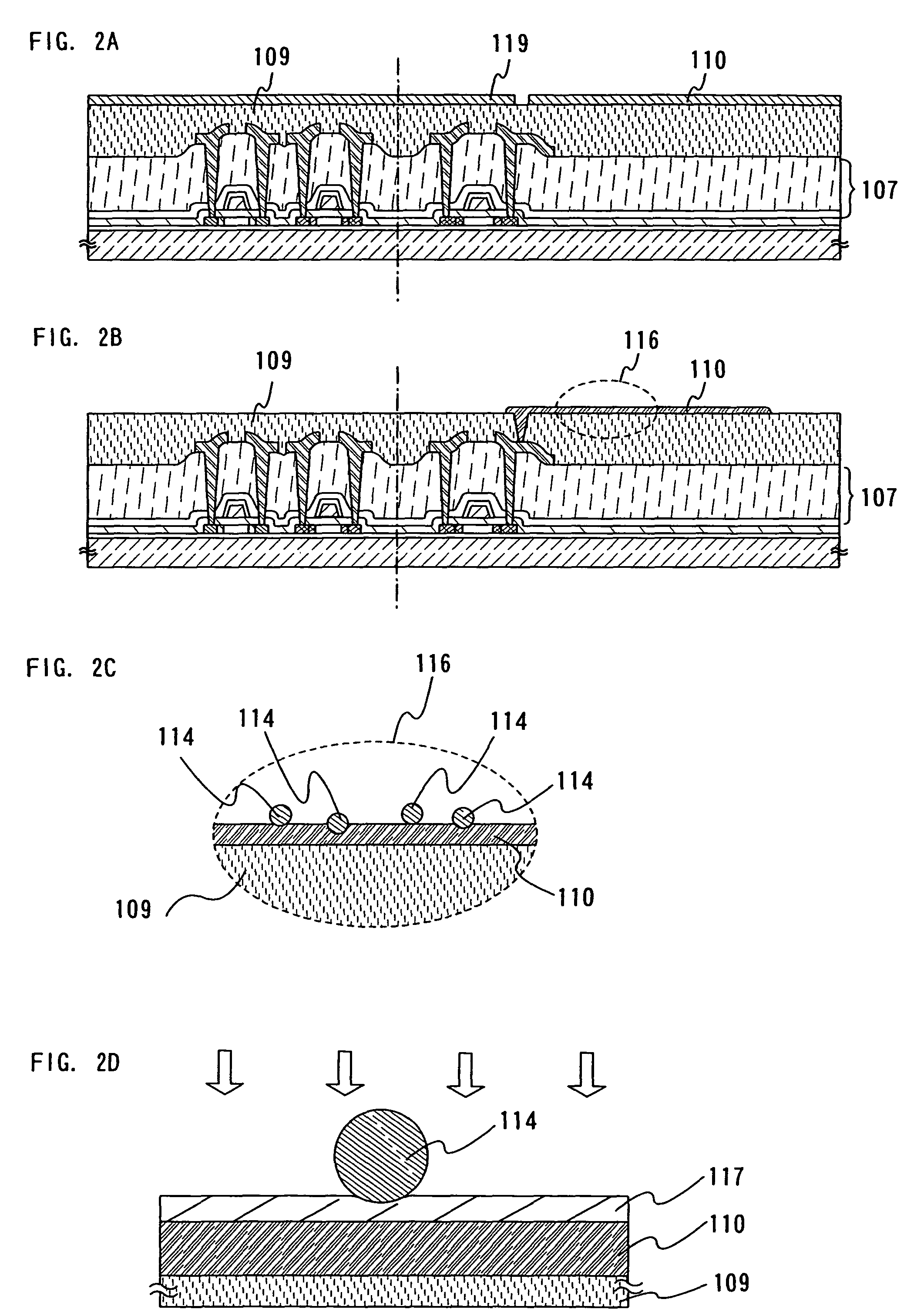
[0045]In this embodiment mode, steps of manufacturing a TFT by using a high-density plasma apparatus will be described with reference to FIGS. 1A to 1E, 2A to 2D, and 15.

[0046]First, as shown in FIG. 1A, a base film 102 is formed over an insulating substrate 101. The insulating substrate 101 can be, for example, a glass substrate such as barium borosilicate glass or alumino borosilicate glass, a quartz substrate, a ceramic substrate, or the like. In addition, a substrate formed of a synthetic resin having flexibility such as a plastic can also be used as long as it can resist a processing temperature in a manufacturing step, although such a substrate generally tends to have a low allowable temperature limit compared with the above substrates. The surface of the insulating substrate 101 may be polished by a CMP method or the like to be planarized. When a glass substrate is used as the insulating substrate 101, the surface of the glass substrate may be nitrided using a high-density pl...

embodiment mode 2

[0082]In this embodiment mode, a method for manufacturing a TFT having a nitride film over a surface of a gate insulating film and a gate electrode by nitriding the gate insulating film and the gate electrode using a high-density plasma apparatus will be described.

[0083]As shown in FIG. 3A, a base film 204 including a first base film 202 and a second base film 203 is formed over an insulating substrate 201. The insulating substrate 201 can be, for example, a glass substrate such as barium borosilicate glass or alumino borosilicate glass, a quartz substrate, a ceramic substrate, or the like. In addition, a substrate formed of a synthetic resin having flexibility such as a plastic can also be used as long as it can resist a processing temperature in a manufacturing step, although such a substrate generally tends to have a low allowable temperature limit compared with the above substrates. The surface of the insulating substrate 201 may be polished by a CMP method or the like to be pla...

embodiment mode 3

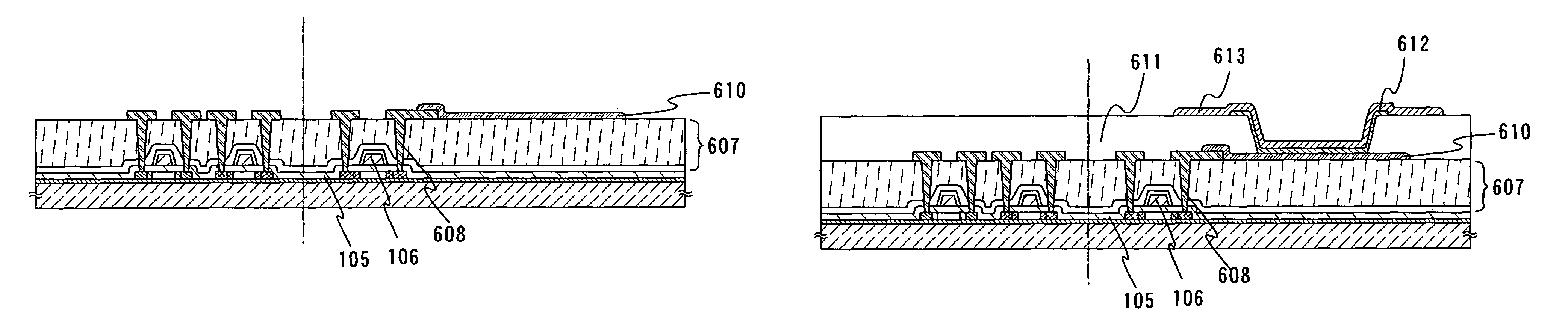
[0097]In this embodiment mode, a method for manufacturing a display device (an EL display device) including an electroluminescence element (hereinafter referred to as an EL element) using the TFT manufactured in Embodiment Mode 1 will be described. Obviously, the TFT manufactured in Embodiment Mode 2 can also be used.

[0098]In this embodiment mode, a first electrode 110 is formed by using a film having a light-transmitting property to have a structure in which light from an electroluminescence element is extracted from the first electrode 110 side. In this embodiment mode, similarly to Embodiment Mode 1, indium tin oxide containing silicon oxide (ITSO) is used as the first electrode 110.

[0099]First, as shown in FIG. 4, an insulating film 111 (referred to as a bank, a partition wall, a barrier, an embankment, or the like) is formed to cover an end portion of the first electrode 110 and the TFT.

[0100]The insulating film 111 can be formed by using silicon oxide, silicone nitride, silico...


PUM


Abstract

In order to manufacture a highly reliable and compact TFT, it is an object of the present invention to provide a method for manufacturing a semiconductor device for forming a gate electrode, a source wiring and a drain wiring with high reliability, and a semiconductor device. In the method for manufacturing a semiconductor device, a semiconductor film is formed over a substrate having an insulated surface, a gate insulating film is formed over the semiconductor film, a gate electrode is formed over the gate insulating film, and a nitride film is formed over the surface of the gate electrode by nitriding the surface of the gate electrode by using high-density plasma.

Description

BACKGROUND OF THE INVENTION[0001]1. Field of the Invention[0002]The present invention relates to a method for manufacturing a semiconductor device, particularly a method for manufacturing a semiconductor device using a high-density plasma apparatus in a manufacturing step of a semiconductor element (device) such as a thin film transistor.[0003]2. Description of the Related Art[0004]In recent years, a technique for forming a thin film transistor (TFT) by using a semiconductor thin film (a thickness of around several nanometers to several hundred nanometers) formed over a substrate having an insulated surface such as glass has been attracting attention. The thin film transistor is broadly applied to semiconductor devices such as an IC and an electro-optic device. In accordance with demands for a more compact and much higher performance semiconductor device, a development of a much higher performance thin film transistor having a minute structure is required. In order to manufacture a ...

Claims


Application Information

Patent Timeline
Patent Type & Authority Patents(United States)
IPC IPC(8): H01L21/336
CPCH01L27/1266H01L27/1248H01L27/1255
Inventor ISOBE, ATSUOMURAKAMI, SATOSHIYAMAZAKI, SHUNPEI
Owner SEMICON ENERGY LAB CO LTD
Why Eureka
Try Eureka