Method for manufacturing a layer arrangement and layer arrangement

a manufacturing method and technology of layer arrangement, applied in the direction of semiconductor devices, semiconductor/solid-state device details, electrical devices, etc., can solve the problems of undesirable crosstalk, high signal propagation time, and high power loss

Inactive Publication Date: 2010-10-05
INFINEON TECH AG
View PDF44 Cites 22 Cited by
  • Summary
  • Abstract
  • Description
  • Claims
  • Application Information

AI Technical Summary

Benefits of technology

[0013]Embodiments of the invention are based on the problem of providing an alternative layer arrangement having air gaps between adjacent interconnects in which undesirable filling of air gaps with dielectric material during the application of a cover layer that covers the interconnects is reliably avoided.
[0021]According to the invention, material of the cover layer is deposited selectively only on those surface regions of the layer sequence which are free of the protective layer (first layer). If that surface region of the layer sequence which is remote from the substrate and is free of the protective layer is shifted far enough toward the top, then after the formation of the cover layer a region between adjacent interconnects that are covered with the thin protective layer remains largely free of dielectric material, whereby air gaps are formed. As a result, an interconnect arrangement having a low value of the dielectric constant is obtained in which parasitic capacitances are low owing to the provision of the air gaps and good shielding and reliable protection against mechanical damage of the sensitive interconnect-air gap structures is achieved owing to the cover layer. An undesirable projection of the cover layer into air gap regions is simultaneously avoided owing to the selectivity of the deposition method for forming the electrically insulating second layer.
[0032]By contrast, the first layer is preferably formed by means of a conformal deposition method, with the result that the first layer then has a constant thickness over the entire layer sequence. This avoids a situation in which (for example, dielectric) material applied to the electrically conductive structures with an uncontrolled thickness possibly closes or fills air gaps between adjacent interconnects in an undesirable manner.
[0037]To put it another way, this material essentially has the favorable dielectric properties of silicon oxide (that is to say a low value of the relative permittivity and hence a low RC switching delay), and the material composition (probably in particular the nitrogen component therein) simultaneously has the effect that the material formed on the basis of an organic precursor has material properties that are rather similar to silicon nitride with regard to the selective deposition of ozone / TEOS.
[0038]This material of the first layer allows a material based on silicon oxide to be used instead of silicon nitride as material between air gaps, without losing the advantages of selective deposition.

Problems solved by technology

As a result, capacitances formed between the interconnects rise and lead to high signal propagation times, high power loss and undesirable crosstalk, that is to say to an interaction between signals applied on adjacent interconnects.
However, a series of problems arise in the production of air gaps.
As a result, there is the risk of a conflict with an overlying metallization level, for example when opening the air gaps in a CMP method step (“chemical mechanical polishing”), see Arnal.
Furthermore, there is a problem with air gap structures in accordance with the prior art in that during the formation of a dielectric cover layer for covering interconnects, dielectric material can pass into regions between adjacent interconnects in an undesirable manner, that is to say can fill air gaps, which runs counter to the formation of an intermetal dielectric having a low k value.

Method used


Image

  • Method for manufacturing a layer arrangement and layer arrangement
  • Method for manufacturing a layer arrangement and layer arrangement
  • Method for manufacturing a layer arrangement and layer arrangement

Examples


Embodiment Construction

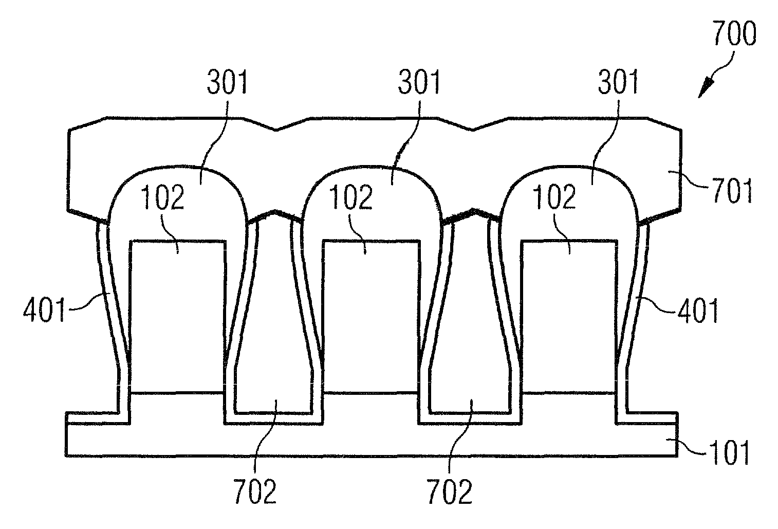
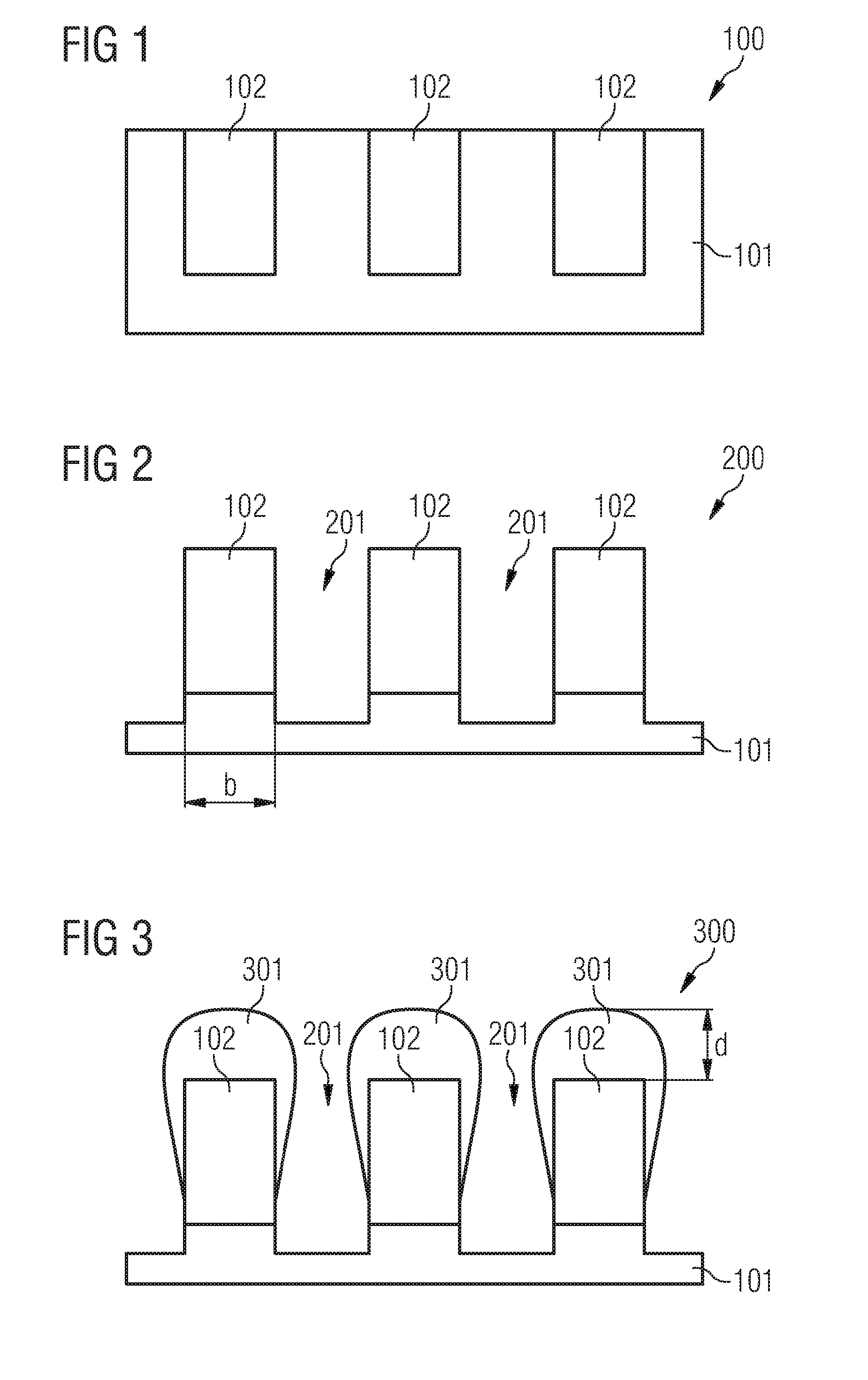
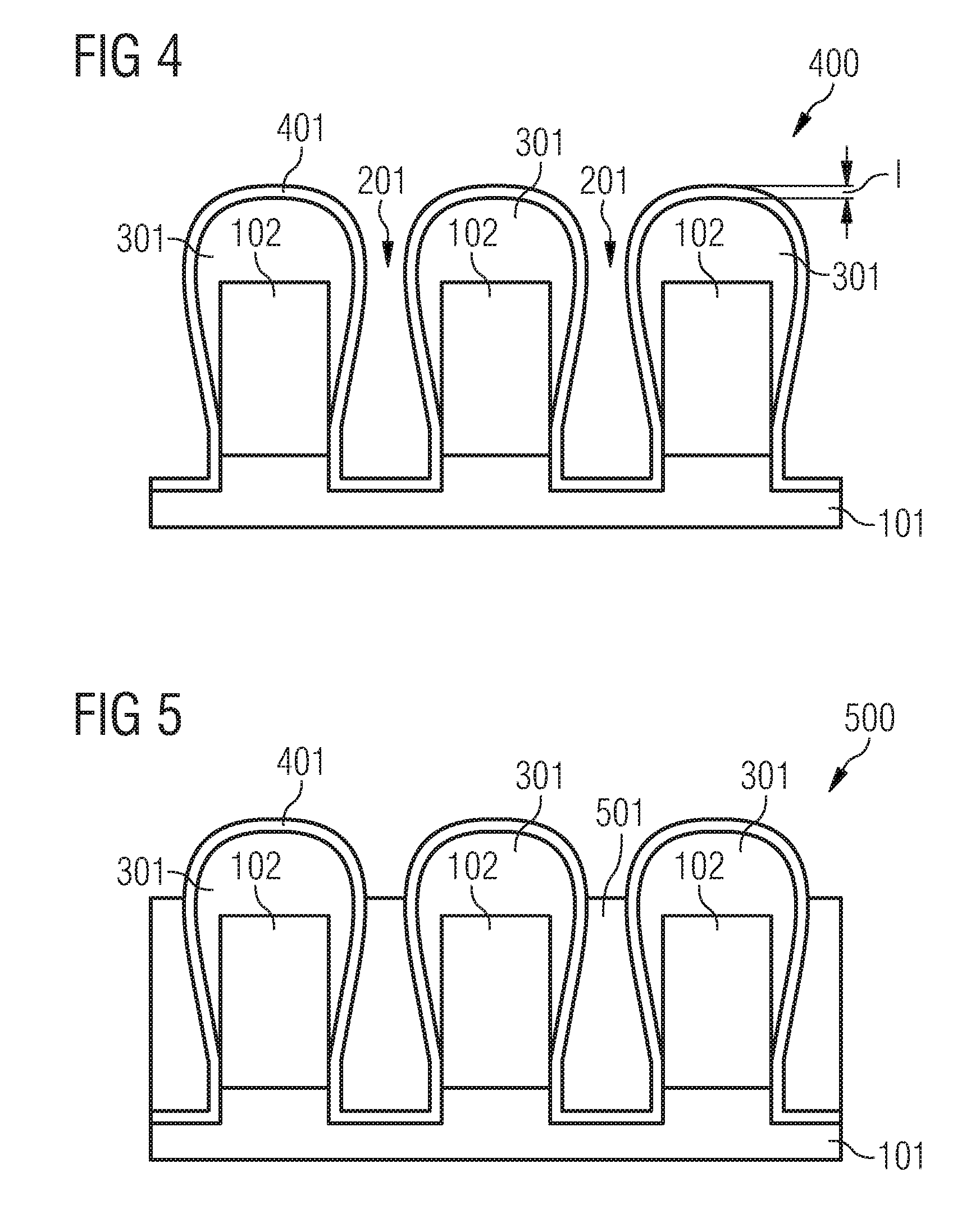
[0080]Identical or similar components in different figures are provided with identical reference numerals.

[0081]A description is given below, referring to FIG. 1 to FIG. 7, of a method for producing a layer arrangement in accordance with a first exemplary embodiment of the invention.

[0082]In order to obtain the layer sequence 100 shown in FIG. 1, trenches are formed on a dielectric substrate 101 (for example composed of silicon oxide material) using a lithography method and an etching method. Copper material is deposited on the layer sequence thus obtained. Material of the deposited copper layer is etched back using a CMP method (“chemical mechanical polishing”), whereby copper interconnects 102 are formed in the trenches. The copper interconnects 102 are therefore produced according to the damascene principle. A diffusion barrier (for example composed of TaN / Ta) not shown in FIG. 1 may be formed between a respective copper interconnect 102 and the substrate 101. A barrier layer may...


PUM


Abstract

In a method for manufacturing a layer arrangement, a plurality of electrically conductive structures are embedded in a substrate. Material of the substrate is removed at least between adjacent electrically conductive structures. An interlayer is formed on at least one portion of sidewalls of each of the electrically conductive structures. A first layer is formed on the interlayer where an upper partial region of the interlayer remaining free of a covering with the first layer. An electrically insulating second layer is formed selectively on that partial region of the interlayer which is free of the first layer, in such a way that the electrically insulating second layer bridges adjacent electrically conductive structures such that air gaps are formed between adjacent electrically conductive structures.

Description

[0001]This application is a continuation of co-pending International Application No. PCT / DE2005 / 001754, filed Sep. 30, 2005, which designated the United States and was not published in English, and which is based on German Application No. 10 2004 050 391.5 filed Oct. 15, 2004, both of which applications are incorporated herein by reference.TECHNICAL FIELD[0002]The invention relates to a method for manufacturing a layer arrangement and a layer arrangement.BACKGROUND[0003]Integrated circuit arrangements are produced with an ever higher packing density. The consequence of this is that interconnects in metallization levels are at an ever smaller distance from one another. As a result, capacitances formed between the interconnects rise and lead to high signal propagation times, high power loss and undesirable crosstalk, that is to say to an interaction between signals applied on adjacent interconnects.[0004]Silicon oxide has a dielectric whose relative permittivity ∈r=3.9 is often used a...

Claims


Application Information

Patent Timeline
Patent Type & Authority Patents(United States)
IPC IPC(8): H01L23/58
CPCH01L21/7682H01L23/5222H01L2924/0002H01L2924/00
Inventor GABRIC, ZVONIMIRPAMLER, WERNERSCHINDLER, GUENTHERSTEINLESBERGER, GERNOTSTICH, ANDREASTRAVING, MARTINUNGER, EUGEN
Owner INFINEON TECH AG
Why Eureka
Try Eureka