

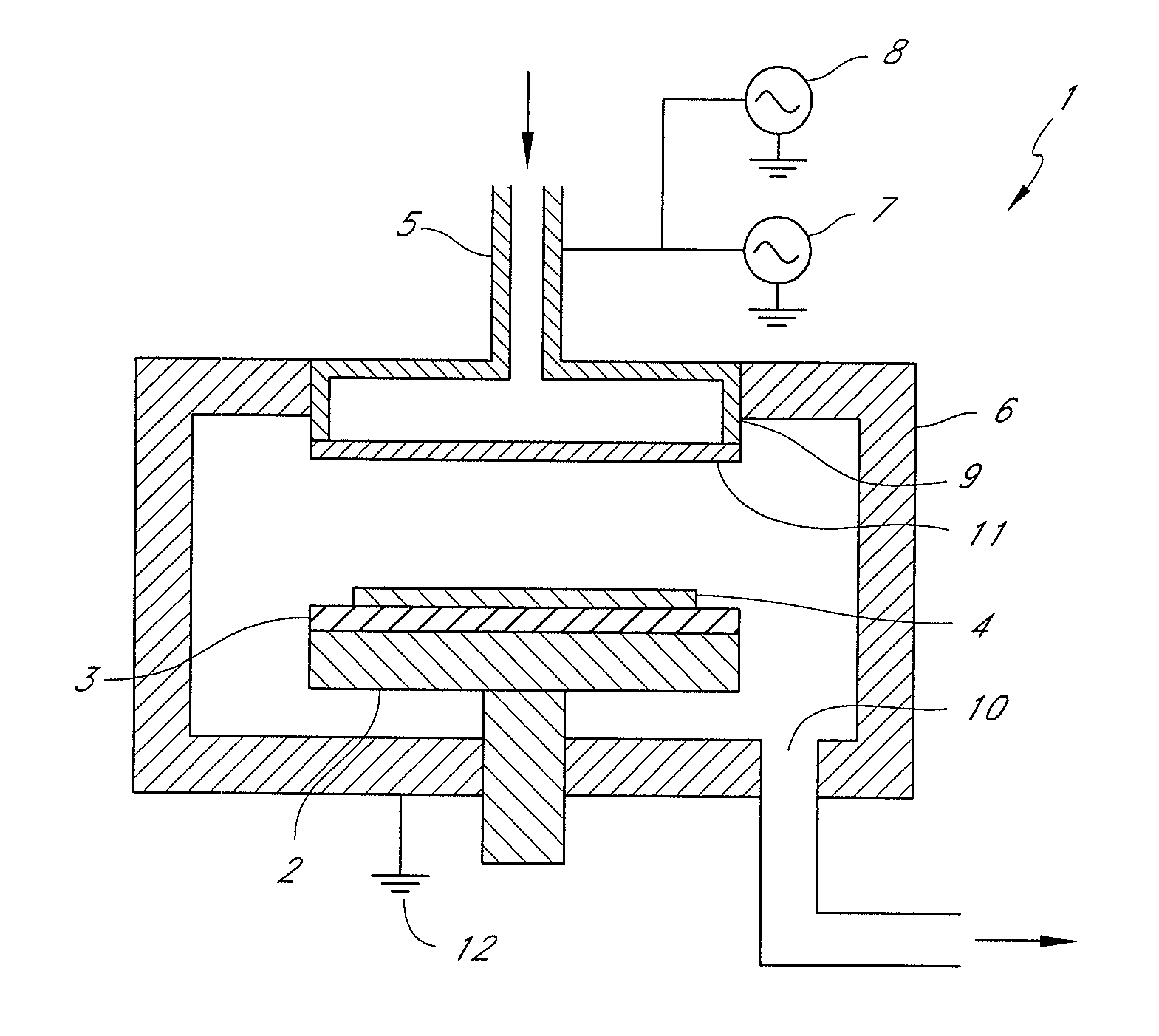
Method for forming dielectric SiOCH film having chemical stability
a technology of dielectric sioch film and chemical stability, which is applied in the field of forming dielectric sioch film having chemical stability, can solve the problems of increasing the dielectric constant, and reducing the thickness of the film, so as to achieve low dielectric constant, high chemical stability, and low cost
- Summary
- Abstract
- Description
- Claims
- Application Information
AI Technical Summary
Benefits of technology
Problems solved by technology
Method used
Image

Examples
example
[0086]In the example, the conditions were set based on the following considerations.
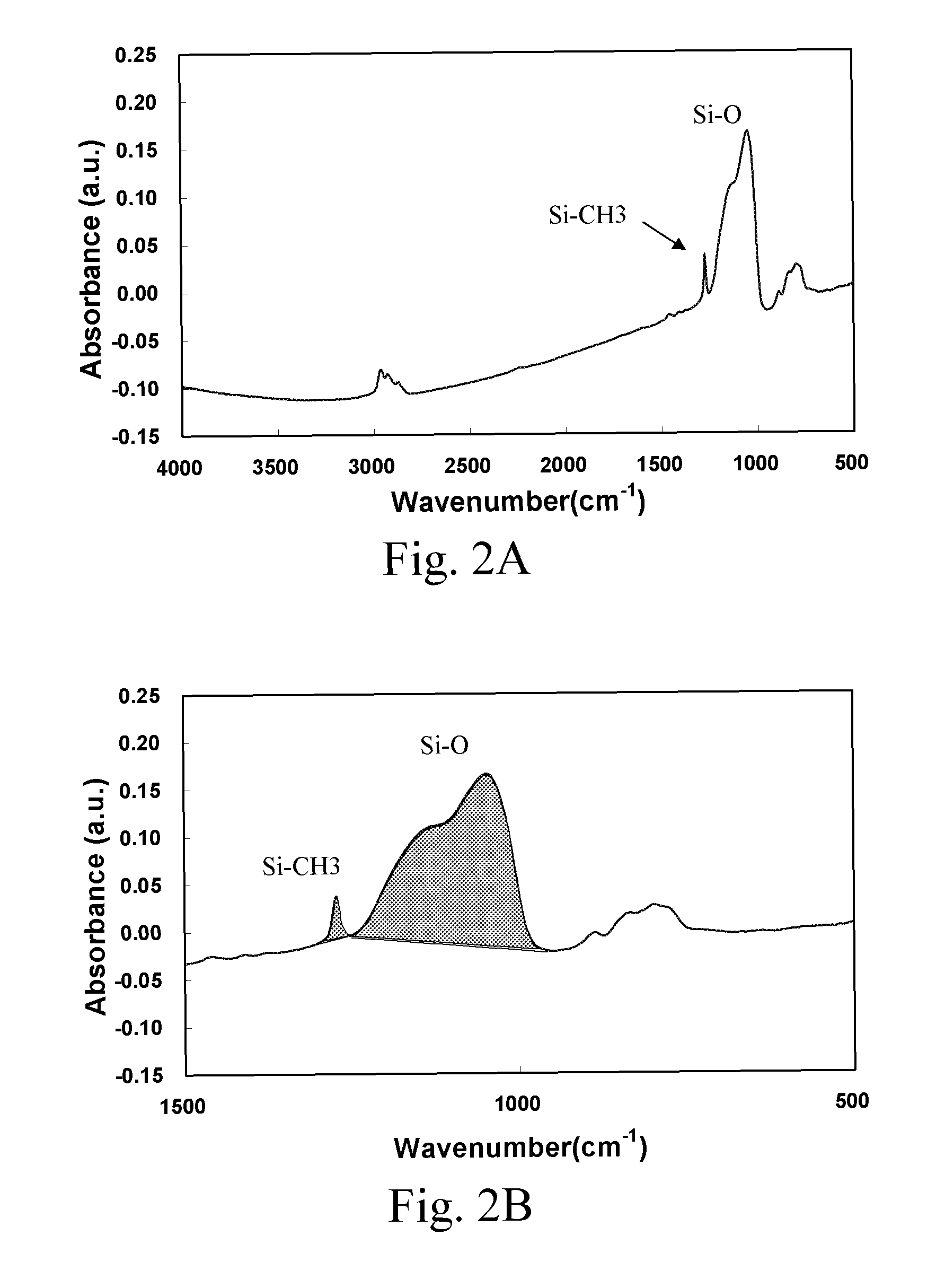
[0087]As the Si—CH3 / Si—O bond strength ratio increases, it is assumed that the percentage of CH3 ends increases relatively at the surface of the SiOCH film. Accordingly, a relative increase in the percentage of CH3 ends leads to an improvement in the chemical stability with respect to chemical solutions due to higher hydrophobicity. On the other hand, increasing the Si—CH3 / Si—O bond strength ratio reduces the elastic modulus.
[0088]Among the parameters that increase the Si—CH3 / Si—O bond strength ratio, changing the film forming conditions / curing conditions in the following manner are effective:
[0089][1] Lower the susceptor temperature.
[0090][2] Widen the Electrode gap.
[0091][3] Lower the RF power.
[0092][4] Shorten the UV curing time.
[0093]In consideration of the above, the film forming conditions / curing conditions were set as follows:
[0094]A: Material gas: DEMS (diethoxy methylsilane) 33 sccm, constan...
PUM
| Property | Measurement | Unit |
|---|---|---|
| elastic modulus | aaaaa | aaaaa |
| dielectric constant | aaaaa | aaaaa |
| time period | aaaaa | aaaaa |
Abstract
Description
Claims
Application Information