
Mm-wave fully integrated phased array receiver and transmitter with on-chip antennas

a phased array, fully integrated technology, applied in the direction of antennas, instruments, antenna feed intermediates, etc., can solve the problems of substrate dielectric loss, difficulty in detecting and the difficulty of coupling power output from an integrated mm-wave transmitter to an off-chip radiating device, etc., to achieve the effect of improving the transmission or reception of mm-waves

Active Publication Date: 2010-10-12
CALIFORNIA INST OF TECH
View PDF7 Cites 131 Cited by
  • Summary
  • Abstract
  • Description
  • Claims
  • Application Information

AI Technical Summary

Benefits of technology

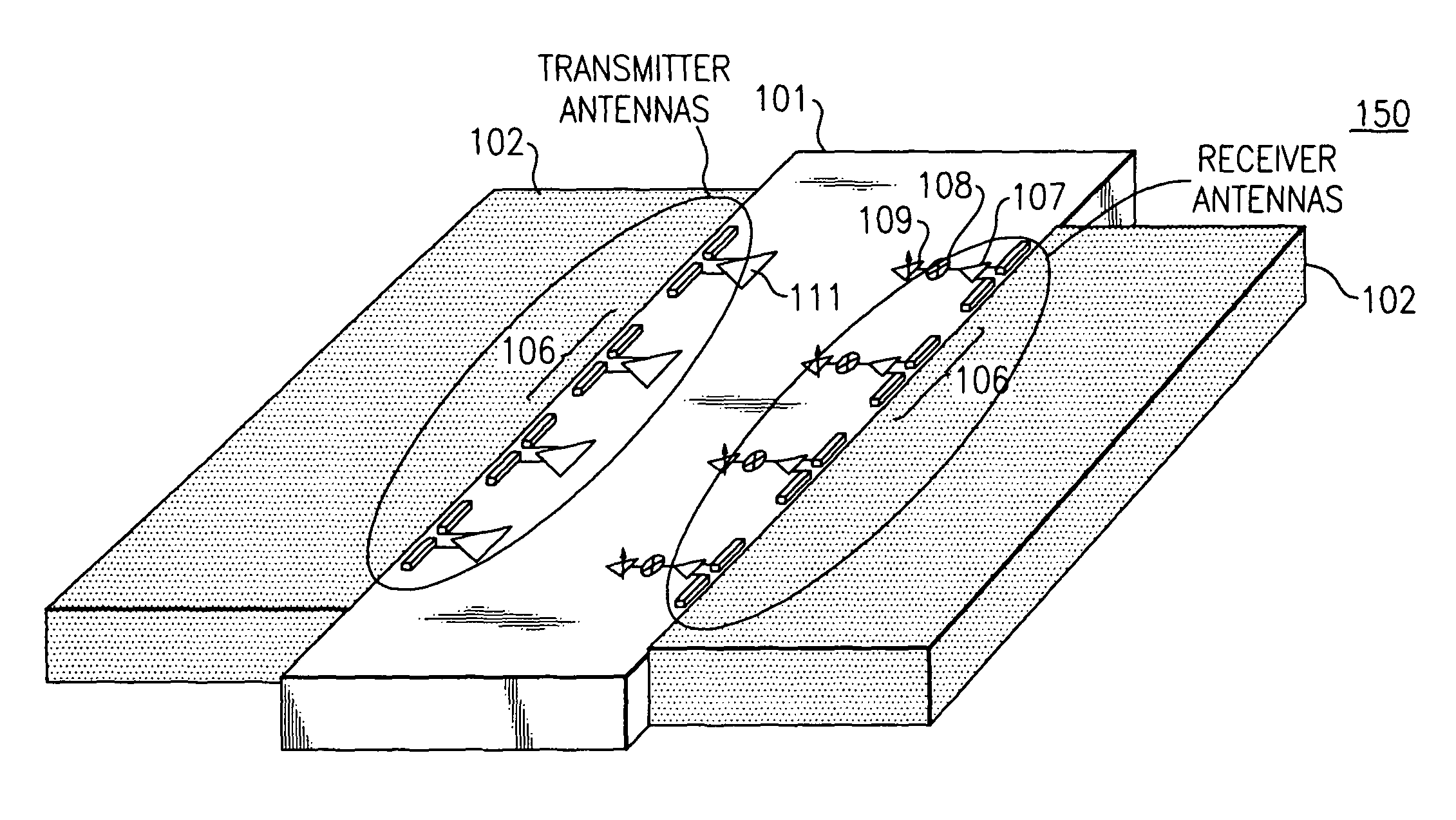
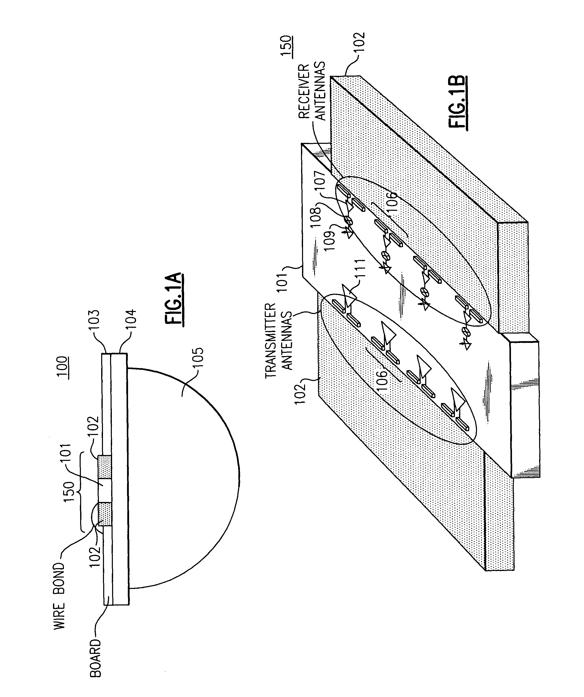
The invention is about a device that uses mm-wave technology to transmit and receive signals. The device includes a substrate and a phased array antenna system with multiple antenna elements. The device also includes a transmitter section and a receiver section, each with a respective phased array antenna system. The antenna elements can be dipole antennas or other types of antennas. The device can be used for voice or data communications, or for radar. The device can be implemented using CMOS or BiCMOS technology. The invention also includes a mm-wave distributed combining tree circuit and a method for measuring the phased array antenna patterns. The technical effects of the invention include improved transmission and reception of mm-wave signals, improved signal-to-noise ratio, and improved performance in millimeter-wave communication and radar applications.

Problems solved by technology

A number of problems have been observed in high frequency mm-wave integrated applications.
Coupling power output from an integrated mm-wave transmitter to an off chip radiating device, such as an off chip antenna, or directly from an integrated circuit emitter to propagation in air is particularly problematic.
Losses related to such off chip coupling can include substrate dielectric loss, substrate conductive losses, voltage induced breakdowns, poor metal conduction to the chip, and unwanted signal radiation at the chip RF interface.
Similar losses, with the exception of voltage induced breakdowns, are problematic when coupling mm-wave signals from the air to the input stages of an integrated mm-wave transceiver.
Another problem involves testing mm-wave integrated devices.
High cost test setups, such as bench instrumentation found in R&D laboratories or automatic test equipment (ATE) as found at production facilities are generally not available for field use.
It is often difficult to properly test and evaluate the performance of most integrated mm-wave applications in the field.

Method used


Image

  • Mm-wave fully integrated phased array receiver and transmitter with on-chip antennas
  • Mm-wave fully integrated phased array receiver and transmitter with on-chip antennas
  • Mm-wave fully integrated phased array receiver and transmitter with on-chip antennas

Examples


example 1

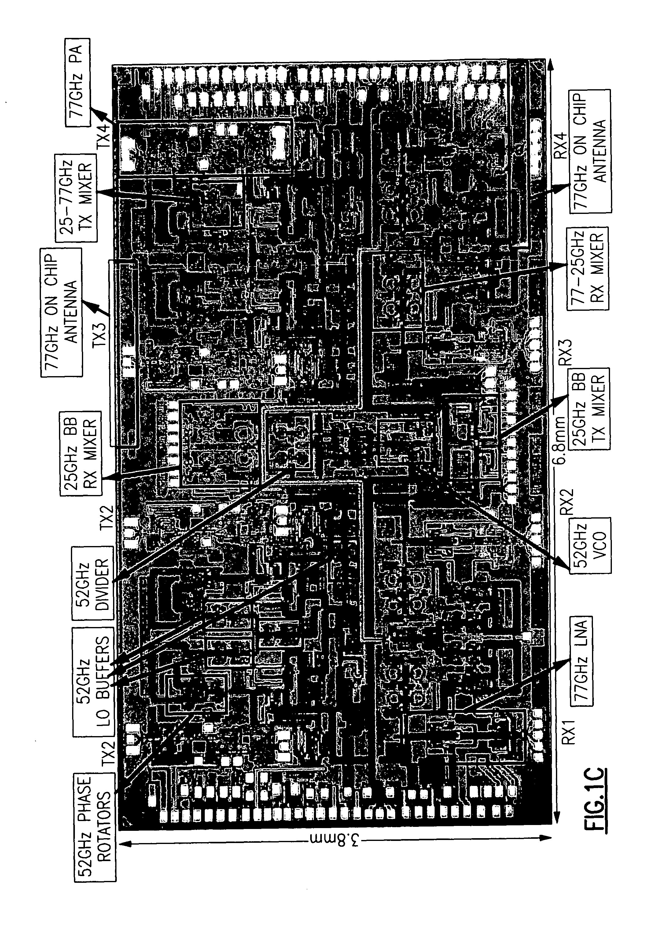
[0094]Several sections of an exemplary mm-wave fully integrated phased array receiver with on-chip antenna are now explained in more detail.

I. Antenna Simulations and Measurement

[0095]IE3D (a MoM-based electromagnetic simulator, available from Zeland Software, Inc., 48834 Kato Road, 103A, Fremont, Calif. 94538; see http: / / www.zeland.com) and HFSS (3D electromagnetic-field simulation software for high-performance electronic design, available from Ansoft Corporation, 225 West Station Square Drive, Suite 200, Pittsburgh, Pa. 15219; see http: / / www.ansoft.com / products / hf / hfss / ) were used to simulate antenna pattern and impedance. The effects of reflection from chip edge, coupling between antenna and its feeding T-lines, metal filling and coupling between adjacent antennas were all simulated. IE3D was used to model the T-lines. FIG. 10 shows an IE3D prototype used to simulate one of the T-line structures of an LNA. The IE3D extracted S-parameters of T-lines can be used in ADS for circuit ...

example 2

[0113]Transmitter chip performance was measured using a combination of waveguide-based probing and self-test mechanisms incorporated in the chip. At all high-frequency measurement points, the pads were incorporated into a tapered coplanar waveguide structure, thereby accounting for pad parasitics while maintaining a 50Ω impedance. For instance, both VCO and divide-by-two outputs were connected to such pad structures to enable direct measurement. The VCO can be tuned from 50.35 GHz to 55.49 GHz, while the locking range of the divider is 51.4 GHz to 54.5 GHz which is sufficient for our application.

[0114]As shown in FIG. 21, a transmitter was characterized using a waveguide probe that was followed by an external downconverter (with a 59 GHz LO). The transmitter generates up to +10.1 dBm output power at 77 GHz and has 34 dB of gain from baseband to RF with a bandwidth of 2.2 GHz.

Loopback Testing

[0115]In order to test the raw beam-performing abilities of the transmitter, excluding the on...

example 3

[0116]FIG. 22A through FIG. 22D show the measured patterns with 2 transmit-receive pairs active in the loopback mode which demonstrates the beam-forming capabilities of the transmitter. The transmitter was implemented in a 0.12 μm SiGe BiCMOS process with seven metal layers. The performance of the phased-array transmitter is summarized in table shown in FIG. 23. The transmitter and local phase shifting occupy 17 mm2 of die area (FIG. 24).


PUM


Abstract

A phased array mm-wave device includes a substrate, a mm-wave transmitter integrated onto the substrate configured to transmit a mm-wave signal and / or a mm-wave receiver integrated onto the substrate and configured to receive a mm-wave signal. The mm-wave device also includes a phased array antenna system integrated onto the substrate and including two or more antenna elements. The phased array mm-wave device also includes one or more dielectric lenses. A distributed mm-wave distributed combining tree circuit includes at least two pairs of differential transconductors with regenerative degeneration and accepts at least two differential input signals. Two mm-wave loopback methods measure the phased array antenna patterns and the performance of an integrated receiver transmitter system.

Description

CROSS-REFERENCE TO RELATED APPLICATIONS[0001]This application claims the benefit and priority of U.S. Provisional Application Ser. No. 60 / 720,228, “A mm-Wave Fully Integrated Phased Array Receiver Transmitter with on Chip Antennas: Receiver with on Chip Antennas”, filed Sep. 23, 2005. The 60 / 720,228 provisional application is hereby incorporated by reference in its entirety. Other aspects of the instant invention are discussed in U.S. patent application Ser. No. 10 / 988,199, “Monolithic Silicon-Based Phased Arrays for Communications and Radars”, filed Nov. 12, 2004. The Ser. No. 10 / 988,199 application, now U.S. Pat. No. 7,502,631 issued Mar. 10, 2009, is hereby incorporated by reference in its entirety.FIELD OF THE INVENTION[0002]The invention relates to mm-wave receivers and transmitters in general and particularly to an integrated mm-wave device that employs a phased array.BACKGROUND OF THE INVENTION[0003]Semiconductor integrated circuit (IC) density and maximum frequency of operat...

Claims


Application Information

Patent Timeline
Patent Type & Authority Patents(United States)
IPC IPC(8): H01Q19/06H01Q15/06
CPCG01S7/032H01Q9/065H01Q19/065G01S7/03
Inventor BABAKHANI, AYDINGUAN, XIANGHAJIMIRI, SEYED ALIKOMIJANI, ABBASNATARAJAN, ARUN
Owner CALIFORNIA INST OF TECH
Learn More