High-speed data sampler with input threshold adjustment

a data sampler and input threshold technology, applied in the field of integrated circuits, can solve the problems of limiting the minimum input signal level that can be successfully resolved, difficulty in accurately resolving received data, and increasing the time required for sampling and resolving data, so as to reduce the effective input offset of the circuit, improve the bandwidth of the receiving circuit, and improve the effect of sampling ra

Inactive Publication Date: 2010-10-12
SLT LOGIC
View PDF41 Cites 86 Cited by
  • Summary
  • Abstract
  • Description
  • Claims
  • Application Information

AI Technical Summary

Benefits of technology

[0007]Optionally, the offset control signal can be adapted to resolve the data signal into an output logic state at a relatively faster rate when a first polarity of the data signal coincides with a first polarity of the offset control signal during a transition of the strobe pulse; and resolve the data signal into an output logic state at a relatively slower rate when the first polarity of the data signal coincides with a second (opposite) polarity of the offset control signal during the transition of the strobe pulse. This embodiment improves the receiving circuit's bandwidth.
[0008]A data sampler circuit for resolving and holding a data signal according to another aspect of the invention includes a first latch circuit that has a latching output for holding a logic state; a clock input electrically coupled to the latch for receiving a clocking signal; and a primary data input electrically coupled to the latch for receiving the data signal to be sampled in response to a transition of a clocking signal appearing at the clock input. A secondary threshold control input electrically coupled to the latch for receiving a threshold signal that selectively adjusts a preference of the first latch circuit for resolving the data signal appearing at the primary data input to a selectable logic state. The latch circuit is adapted to resolve the data signal into one of at least two logic states based in part on the threshold signal in response to a clocking signal transition. The threshold signal can be used to reduce the circuit's effective input offset, and to assist in driving the sampling latch's output more quickly to a fully resolved state.

Problems solved by technology

The process of sampling and resolving the data takes an increasingly significant amount of time as the data transmission rates increase.
One problem associated with receiving high data rates is the difficulty with accurately resolving the received data.
However, signal receiving circuits can exhibit a substantial input offset voltage that directly limits the minimum input signal level that can be successfully resolved by the sampling circuit.

Method used


Image

  • High-speed data sampler with input threshold adjustment
  • High-speed data sampler with input threshold adjustment
  • High-speed data sampler with input threshold adjustment

Examples


Embodiment Construction

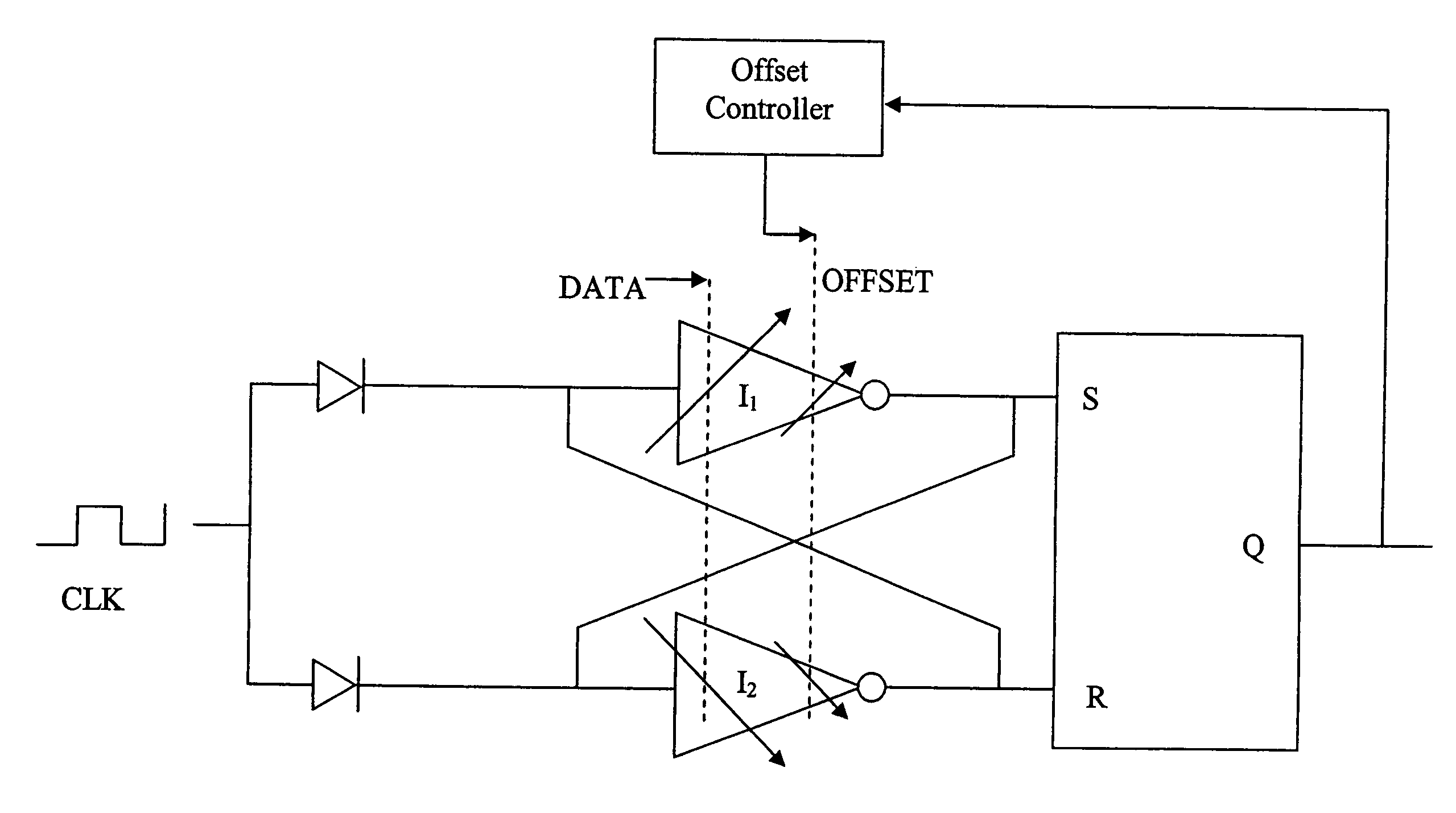
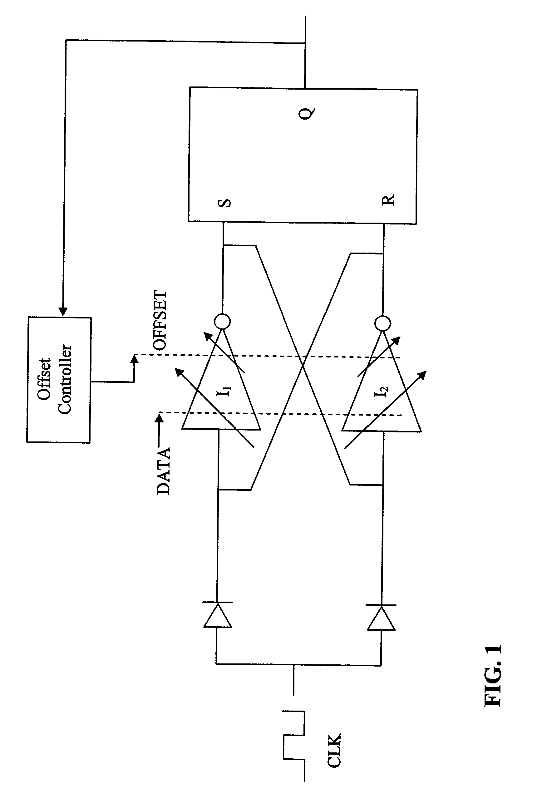
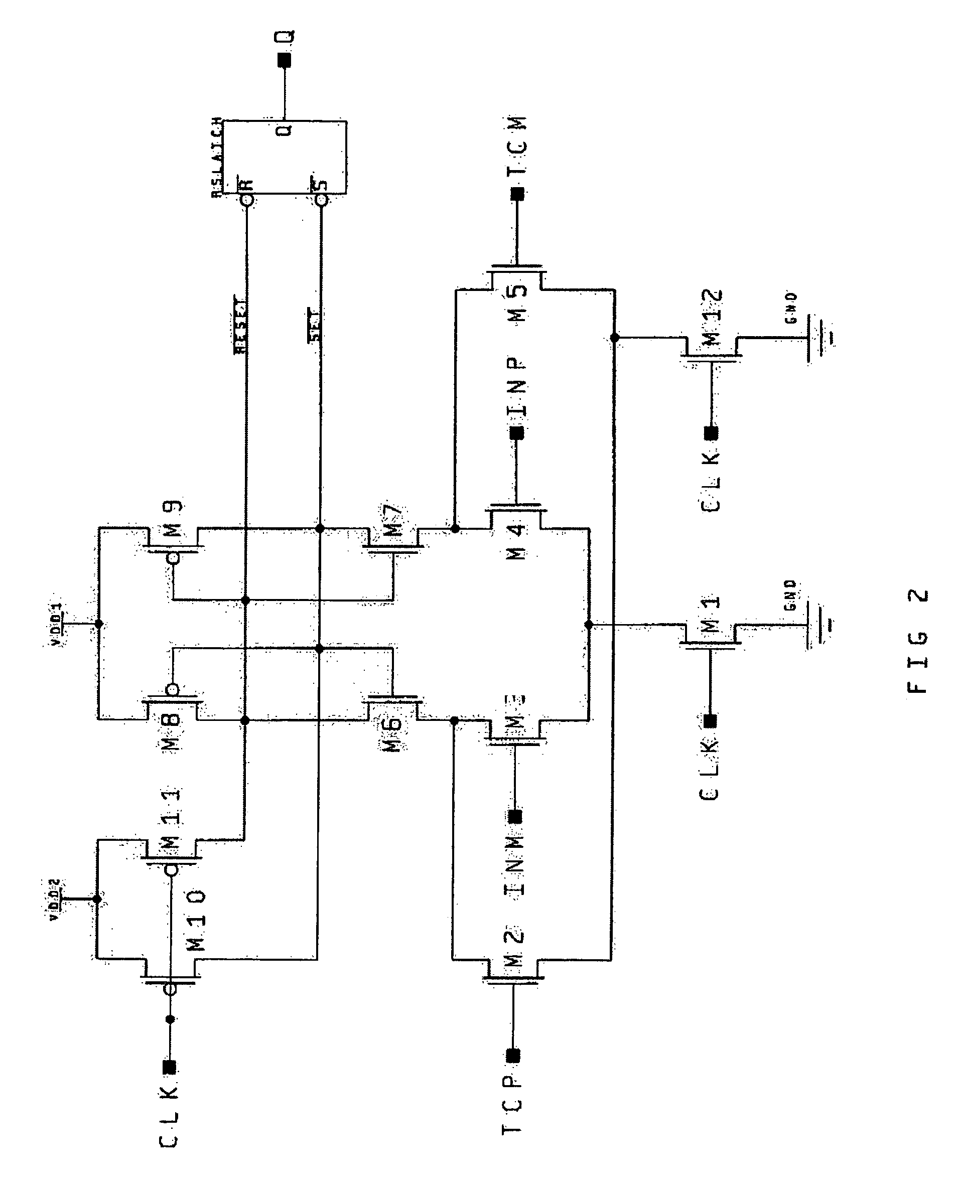
[0012]One aspect of the present invention provides a circuit for adjusting the input threshold voltage of a data sampling circuit used in systems such as those used for high-speed networking, A / D converters, or for clock and data recovery. FIG. 1 is a simplified diagram illustrating an example data latch having two sets of inputs that affect the resolving of data. The data latch includes a first stage latch and a second stage latch. The first stage latch is a strobe-type latch having a matched pair of cross-coupled inverting gates I1 and I2. Although inverting gates I1 and I2 are depicted in FIG. 1 as inverters, persons skilled in the art will recognize that any suitable type of circuit can be substituted within the spirit of the invention including, but not limited to, NAND gates, NOR gates, and the like. The second stage latch is an RS-type latch.

[0013]When the clocking signal CLK is low, the first stage latch of FIG. 1 maintains a latched state using the positive feedback of the ...


PUM


Abstract

Method and apparatus for sampling a high-speed digital signal include providing a data signal to a differential data input circuit, an offset control signal, and a strobe pulse. In response to the strobe pulse, the data signal is resolved into an output logic state based to a relatively greater extent on the differential data signal and to a relatively lesser extent on the offset control signal.

Description

THE FIELD OF THE INVENTION[0001]The present invention generally relates to integrated circuits, and more particularly to data samplers and data sampling circuits, and circuits for adjusting the input threshold of data sampling circuits, especially at high speeds such as rates above 0.10 Gb / s.BACKGROUND OF THE INVENTION[0002]Certain methods of receiving high speed data signals involve sampling an incoming data stream and determining the logic state of each symbol period of the incoming signal. Based on the determined logic state, the data stream is re-generated locally for further processing. The process of determining and re-generating the sampled logic state is known in the art as resolving the logic state. The process of sampling and resolving the data takes an increasingly significant amount of time as the data transmission rates increase. At rates above 10 Gb / s, the sampling and re-generating time becomes a bottleneck, and a solution for improving the data resolving time is need...

Claims


Application Information

Patent Timeline
Patent Type & Authority Patents(United States)
IPC IPC(8): H04L7/00H04J3/06H03L7/00H04J3/07
CPCH03K3/356139H04L25/063
Inventor FIEDLER, ALAN
Owner SLT LOGIC
Why Eureka
Try Eureka