Semiconductor storage device

a technology of semiconductors and storage devices, applied in the direction of information storage, static storage, digital storage, etc., can solve the problems of data-write errors, data-read errors, data-read errors,

Inactive Publication Date: 2010-10-19
SOCIONEXT INC
View PDF14 Cites 4 Cited by
  • Summary
  • Abstract
  • Description
  • Claims
  • Application Information

AI Technical Summary

Benefits of technology

[0019]Therefore, a main object of the present invention is to step down a potential of a bit line to an optimal level without being affected by variability in devices or operation conditions.
[0027]According to the constitution provided by the present invention, wherein the step-down level is adjusted in accordance with the potentials (charge amount) of the bit lines, the potential of any bit line can be stepped down to the same level without being affected by variability in pulse widths of the step-down control signal and load capacities of each bit line and the like.
[0028]Further, a transistor of an optical dummy pattern in which the monitor circuit is provided in the periphery of the memory cell array is used, which makes it unnecessary to provide the step-down circuit as a peripheral circuit. As a result, the circuit layout area can be reduced.
[0029]Further, the activation of the word line is prohibited by the intermediate step-down control signal issued by the bit line potential monitor circuit, which can prevent the occurrence of such an unfavorable event that the word line is activated though the step-down level is not sufficient, and the data of the memory cell is thereby destroyed. Alternatively, the activation of the word line is attenuated when the step-down level is insufficient, which prevents the bit-line current from rapidly flowing into the memory cell. As a result, the destruction of the data in the memory cell can be prevented.

Problems solved by technology

However, when a step-down level in the bit line is below the operation region of a transistor for detection, through current and a data-read error may occur.
A data-read error also occurs in the case where a sense amplifier or a PMOS cross driver is connected to the bit line.
The inflow of too many charges results in the occurrence of a data-write error.
In the case where a step-down of the bit line is not enough, a data-write error occurs due to the reason described above.
On the other hand, in the case where the step-down is excessive, a data-write error is caused by charges of “L” level of the bit line which flow into the node of the SRAM at which “H” data is retained.
Therefore, when the pulse width Tw of the step-down control signal DC is changed due to operation conditions or variability in devices, a large difference is generated in the step-down level ΔV, which results in malfunctioning.
As a result, it is increasingly difficult to compensate for the step-down level in the bit line.
Further, a bit line step-down circuit and control circuit which controls the step-down operation occupy a larger area, as a result of which a circuit layout area and a reading speed are unfavorably increased.

Method used


Image

  • Semiconductor storage device
  • Semiconductor storage device
  • Semiconductor storage device

Examples


embodiment 1

Preferred Embodiment 1

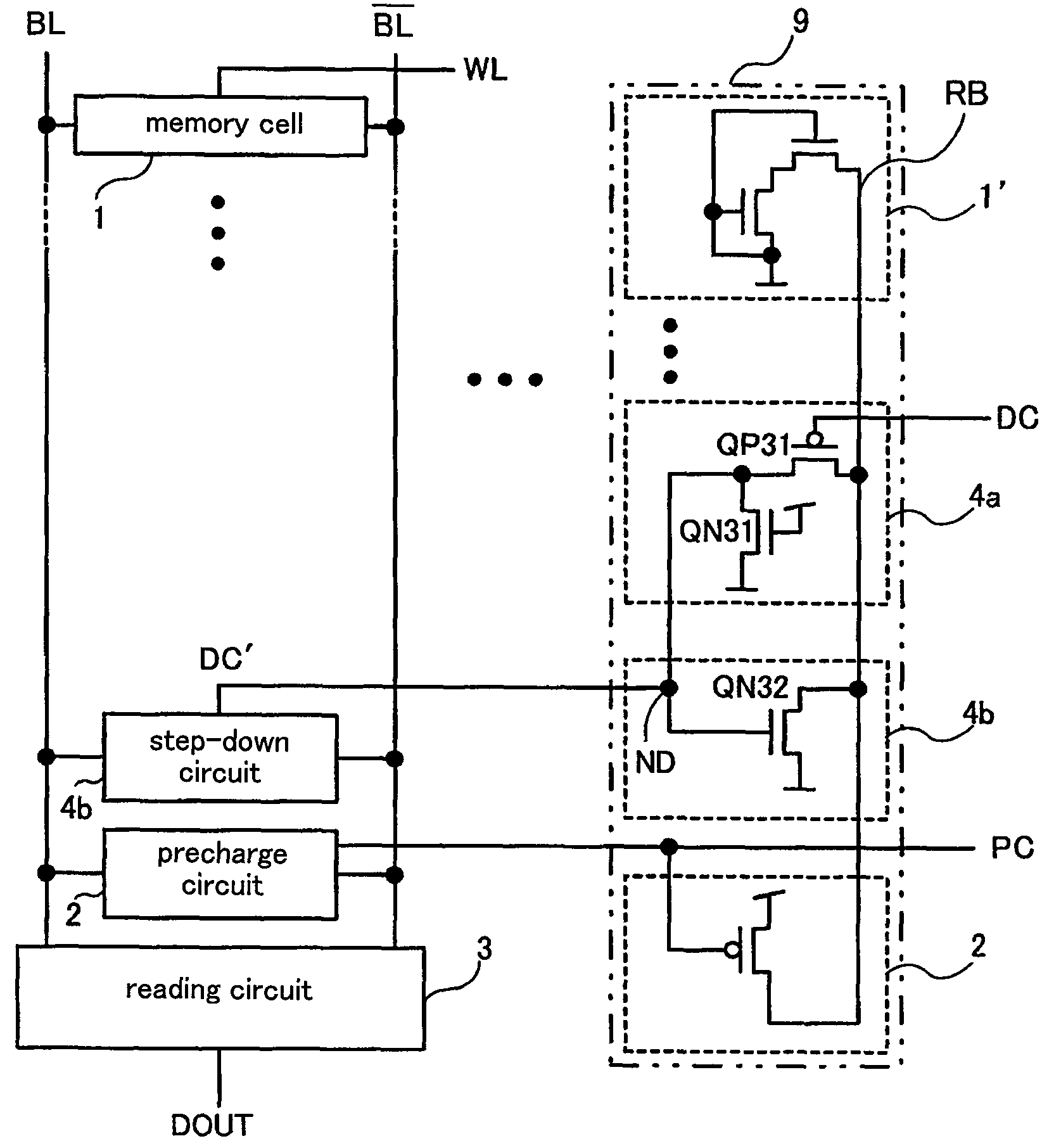
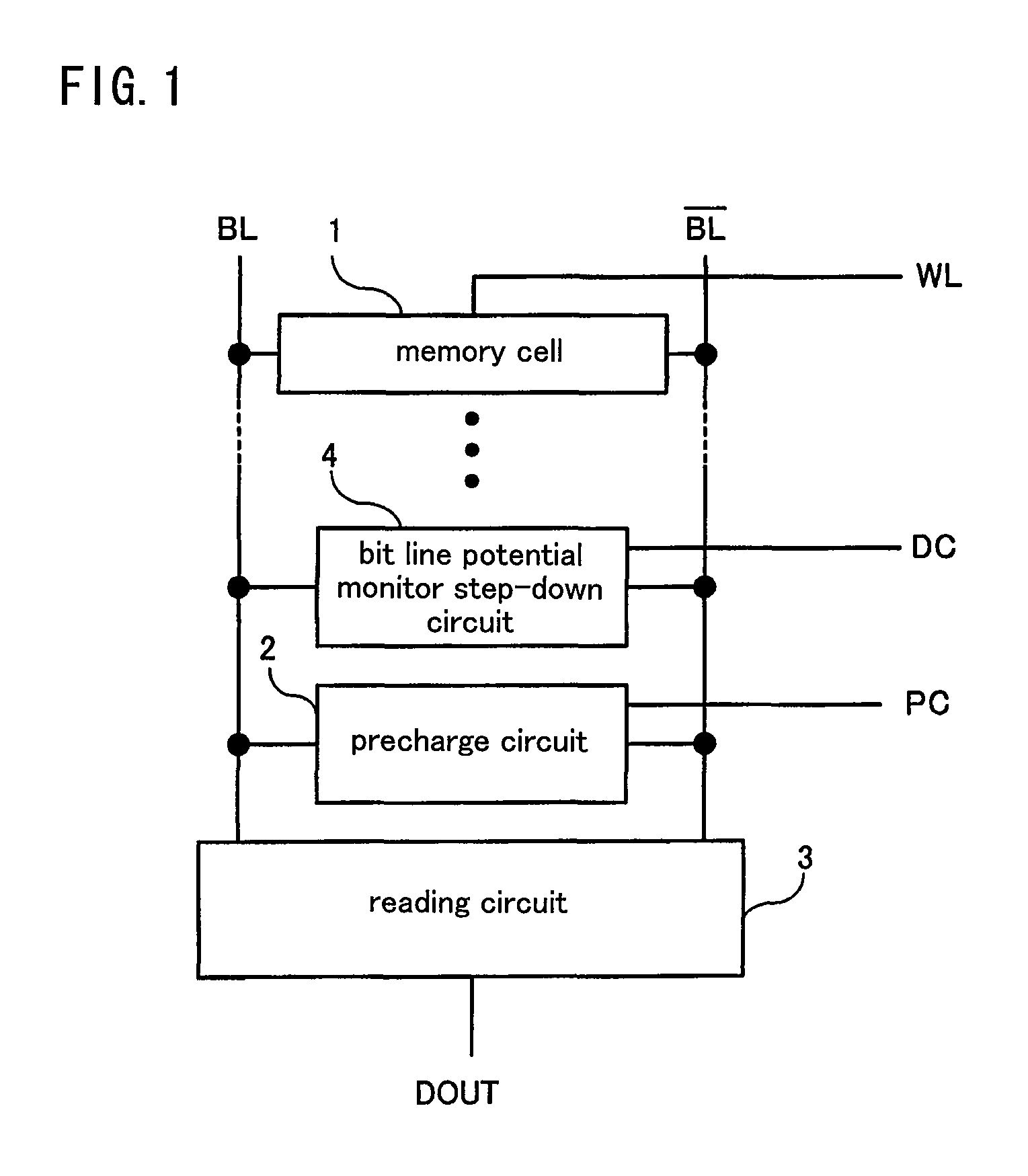
[0061]FIG. 1 is a circuit diagram illustrating a constitution of a semiconductor storage device according to a preferred embodiment 1 of the present invention. The semiconductor storage device according to the present preferred embodiment comprises a memory cell 1, which is SRAM (Static Random Access Memory) activated when accessed via a word line WL, bit lines BL and BL− connected to the memory cell 1 which transmit potentials necessary for writing and reading data, and a bit line potential monitor step-down circuit 4 which monitors the potentials of the bit lines BL and BL− and adjusts step-down levels of the bit lines BL and BL− in accordance with the monitored potentials of the bit lines BL and BL−.

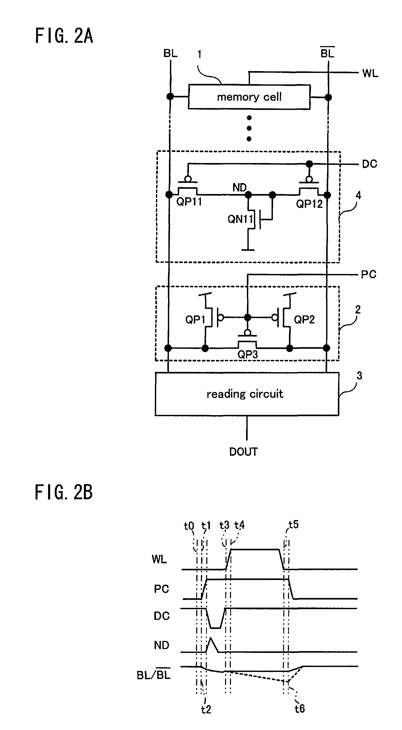
[0062]FIGS. 2A and 2B respectively illustrate a specific example of a circuit and a timing chart thereof. As illustrated in FIG. 2A, the precharge circuit 2 comprises switching transistors QP1 and QP2 which are PMOS transistors as switching elements for precharge...

embodiment 2

Preferred Embodiment 2

[0076]FIG. 3 illustrates a circuit configuration of a semiconductor storage device according to a preferred embodiment 2 of the present invention. In FIG. 3, the same reference symbols as those shown in FIG. 2 according to the preferred embodiment 1 denote the same components. The present preferred embodiment is characterized in that an equalizing transistor QP13 is provided. A PMOS transistor constitutes the equalizing transistor QP13. A gate of the equalizing transistor QP13 is connected to the step-down control node ND, and a source and a drain thereof are connected to the bit lines BL and / BL−. The equalizing transistor QP13, which is brought into conduction when the step-down control signal DC is at “L” level, can equalize the potentials of the bit lines BL and / BL− during the step-down for the bit lines BL and / BL−. The rest of the constitution and the operation, which is similar to that of the preferred embodiment 1, is not described again.

embodiment 3

Preferred Embodiment 3

[0077]FIG. 4A illustrates a circuit configuration of a semiconductor storage device according to a preferred embodiment 3 of the present invention, and FIG. 4B is a timing chart of an operation thereof. The present preferred embodiment is characterized in that a precharge and bit line potential monitor step-down circuit 5, which is the combination of the bit line potential monitor step-down circuit 4 and the precharge circuit 2 illustrated in FIG. 3, is provided. In this constitution, NMOS step-down transistors QN12 and QN13, which are serially provided in two stages, are connected to between the step-down control node ND and the ground in place of the step-down transistor QN11 illustrated in FIG. 3. Further, a PMOS precharge transistor QP14 is connected to between the step-down control node ND and the power supply voltage. The step-down control node ND is inputted to the step-down transistor QN12, and a precharge / step-down control signal PDC is inputted to the...


PUM


Abstract

A bit line potential monitor circuit is provided in a bit line, and a step-down circuit of the bit line is controlled base on information from the monitor circuit. As a result, the bit line is easily stepped down to an optimal potential level in accordance with a potential and a load capacity thereof without being affected by variability in devices or operation conditions.

Description

BACKGROUND OF THE INVENTION[0001]1. Field of the Invention[0002]The present invention relates to a semiconductor storage device comprising a memory cell, a bit line connected to the memory cell, and a step-down circuit which steps down a potential of the bit line up to a predetermined voltage level lower than a power supply voltage before data is read from the memory cell.[0003]2. Description of the Related Art[0004]In the field of a semiconductor storage device, there is a conventional technology in which, for the purpose of improving a data reading speed, a bit line precharged with a power supply voltage is stepped down up to a predetermined voltage level lower than the power supply voltage before data is read, so that a period of time required for a voltage level in the bit line to change from the power supply voltage level to the ground level is shortened. The change from the power supply voltage level to the ground level in the bit line is detected by a PMO transistor provided ...

Claims


Application Information

Patent Timeline
Patent Type & Authority Patents(United States)
IPC IPC(8): G11C11/416
CPCG11C11/419
Inventor KOIKE, TSUYOSHI
Owner SOCIONEXT INC
Why Eureka
Try Eureka