Drive circuit

a drive circuit and level shift technology, applied in logic circuit coupling/interface arrangement, pulse generator, pulse technique, etc., can solve the problems of excessive breakdown voltage margin, increase cost, and complicated process, and achieve the effect of reducing the breakdown voltage margin of the power switching element of the drive-stage circui

Inactive Publication Date: 2005-01-18
PANASONIC CORP
View PDF6 Cites 26 Cited by
  • Summary
  • Abstract
  • Description
  • Claims
  • Application Information

AI Technical Summary

Benefits of technology

According to the present invention described above, tho drive circuit can output the output amplitude roughly twice as high as the breakdown voltages, and thereby can sufficiently drive the power switching element even when the drive circuit composes the ampli

Problems solved by technology

However, this complicates the process and also increases the cost.
In this case, however, the power switching element of the drive-stage circuit has an excessively large breakdown voltage margin.
Thi

Method used


Image

  • Drive circuit
  • Drive circuit
  • Drive circuit

Examples


embodiment 1

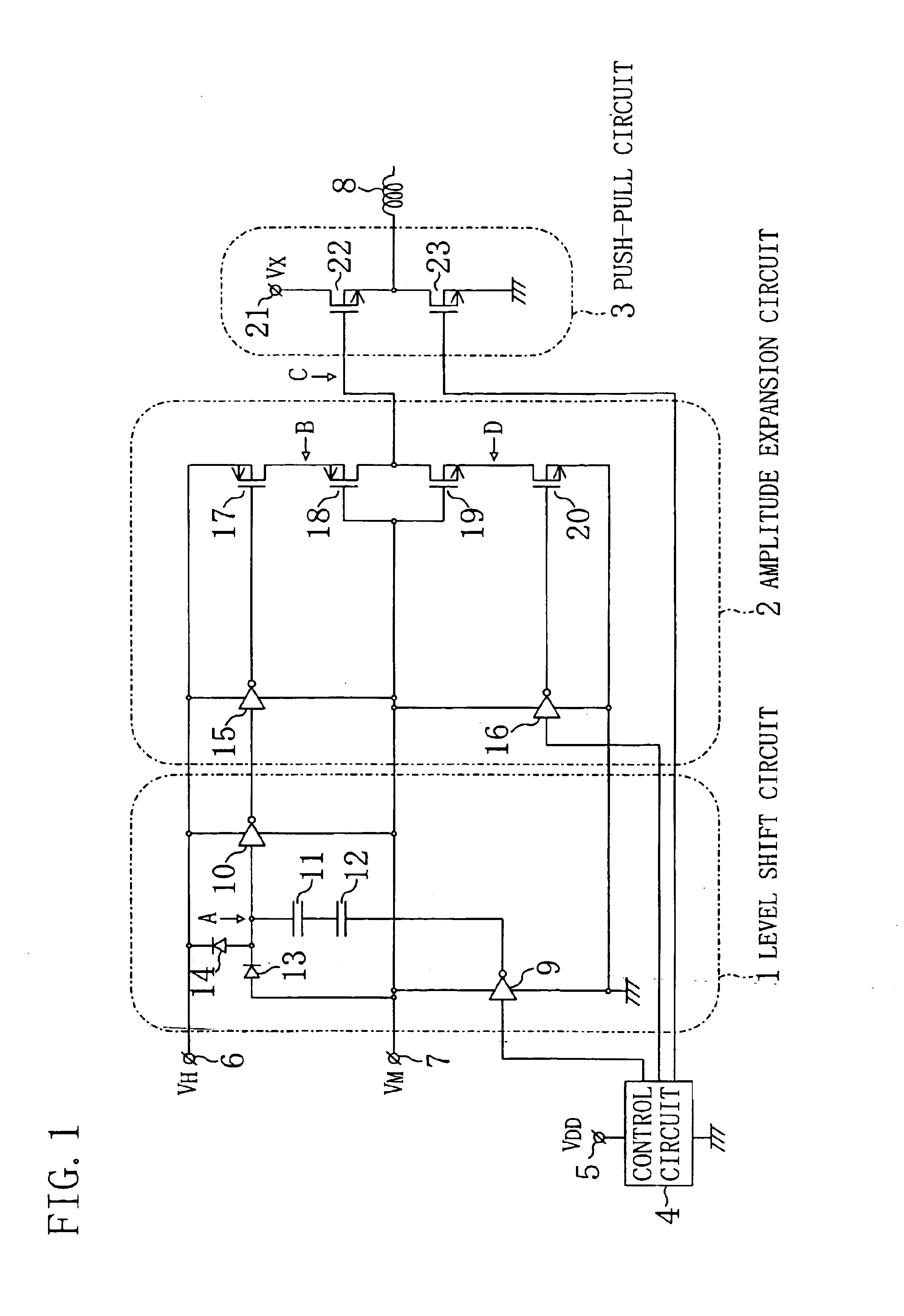
FIG. 1 illustrates a PWM drive circuit of Embodiment 1, which includes a level shift circuit 1, an amplitude expansion circuit 2, and a push-pull circuit 3 as a drive-stage circuit. FIG. 1 also shows components outside the PWM drive circuit, which are a control circuit 4 for controlling the level shift circuit 1, the amplitude expansion circuit 2 and the push-pull circuit 3, a VDD power supply line 5 for supplying a DC voltage VDD, a VH power supply line 6 (second DC power supply line) for supplying a DC voltage VH (second potential), a VM power supply line 7 (intermediate power supply line) for supplying a DC voltage VM (intermediate potential), a ground line (first DC power supply line) connected to the ground, and a load 8 such as a motor and an actuator. The DC voltage VDD, the same voltage as that of the VDD power supply line 5, is applied to the VM power supply line 7, while a voltage roughly twice as high as the DC voltage VM is applied to the VH power supply line 6. Herein, ...

embodiment 2

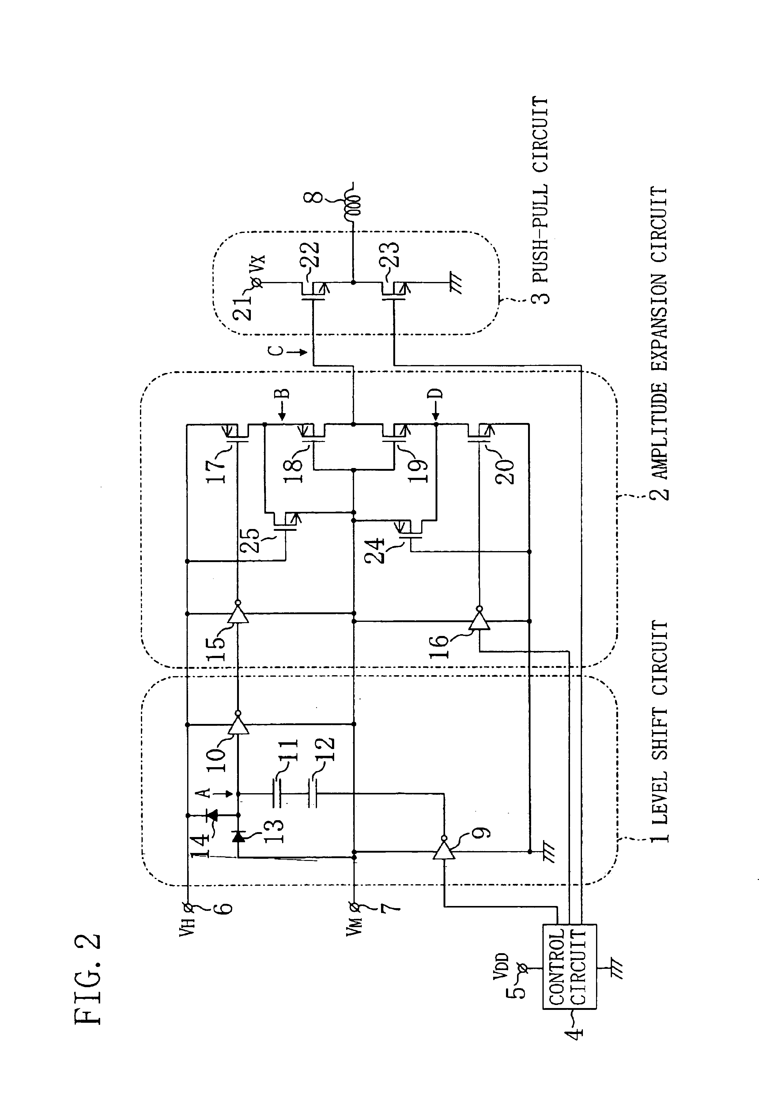
FIG. 2 illustrates a drive circuit of Embodiment 2 of the present invention. In FIG. 2, the following components are added to the configuration shown in FIG. 1. That is, the amplitude expansion circuit 2 additionally includes a p-channel MOSFET 24 (sixth MOSFET of one conductivity) and an n-channel MOSFET 25 (fifth MOSFET of the other conductivity). Hereinafter, these additional components will be described.

As described in Embodiment 1, the CMOS inverter circuit 10 of the level shift circuit 1 outputs a level-shifted signal oscillating between the voltage VH and the voltage VM. The CMOS inverter circuit 15 receives this level-shifted signal, while the CMOS inverter circuit 16 receives a pulse signal with the VDD amplitude from the control circuit 4.

Suppose the CMOS inverter circuit 15 receives a signal of the voltage VH level and the CMOS inverter circuit 16 receives a signal of the voltage VM level. Then, the CMOS inverter circuit 15 outputs the voltage VM and the CMOS inverter cir...

embodiment 3

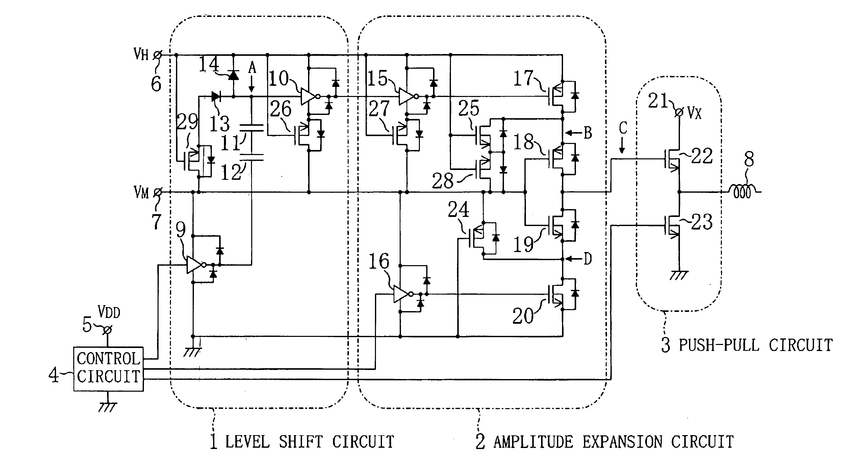
FIG. 3 illustrates a PWM drive circuit of Embodiment 3 of the present invention. In FIG. 3, n-channel MOSFETs 26, 27, 28 and 29 (ninth, seventh, eighth and tenth MOSFETs of the other conductivity) are added to the configuration shown in FIG. 2. In FIG. 3, also, parasitic diodes are depicted for the respective MOSFETs and inverters. Note that the position of each parasitic diode is based on the assumption that the p-well potential of each n-channel MOSFET can be handled independently using a process of forming an n-type layer between the p-well potential and a p-type substrate of the n-channel MOSFET, an insulation separation process or an SOI process.

As described before, as the order of application of the power supply voltages for prevention of breakdown, the power supply voltage VM is first applied to the VM power supply line 7, and then the power supply voltage VH is applied to the VH power supply line 6. In this relation, in the state where a voltage has been applied to the VM po...


PUM


Abstract

The amplitude expansion circuit as a main part of a drive circuit includes: a VM DC power supply line to which a voltage VM is applied; a VH DC power supply line to which a voltage VH roughly twice as high as the voltage VM is applied; an inverter circuit receiving a pulse signal oscillating between the ground voltage and the voltage VM; another inverter circuit receiving a pulse signal oscillating between the voltage VM and the voltage VH in correspondence with the oscillation of the voltage level of the above pulse signal; a p-channel MOSFET having a gate receiving an output from the inverter circuit; another p-channel MOSFET having a gate connected to the VM DC power supply line; an n-channel MOSFET having a gate connected to the VM DC power supply line; and another n-channel MOSFET having a gate receiving an output from the other inverter circuit. A common connection node of the p-channel MOSFET and the n-channel MOSFET works as the output terminal of the amplitude expansion circuit.

Description

BACKGROUND OF THE INVENTIONThe present invention relates to a level shift circuit, an amplitude expansion circuit, and a drive circuit using these circuits.In recent years, pulse width modulation (PWM) drive circuits have been often used for drive control of motors and actuators. To sufficiently turn on a power switching element of a push-pull circuit as a drive-stage circuit at the final stage, a predrive circuit preceding the push-pull circuit is required to output a voltage sufficiently higher than the power supply voltage for the push-pull circuit. For this purpose, the predrive circuit is normally formed using MOSFETs sufficiently high in breakdown voltage. With an output voltage from the predrive circuit, the gate voltage of the power switching element connected to a motor or an actuator is controlled, and by this control, PWM drive of the motor or the actuator is realized.A conventional PWM drive circuit will be described with reference to FIG. 5. A PWM drive circuit shown in...

Claims


Application Information

Patent Timeline
IPC IPC(8): H03K17/10H03K17/06
CPCH03K17/063H03K19/00315H03K17/102
Inventor YAMAMOTO, YASUNORIIWANAGA, TAISHI
Owner PANASONIC CORP
Why Eureka
Try Eureka