Display device

a technology of a display device and a connector is applied in the field of display devices, which can solve the problems of increasing lowering and inferior properties of the transistor, so as to reduce increase the cost of implementation, and reduce the reliability of the connecting par

Inactive Publication Date: 2005-01-20
SEMICON ENERGY LAB CO LTD
View PDF27 Cites 32 Cited by
  • Summary
  • Abstract
  • Description
  • Claims
  • Application Information

AI Technical Summary

Benefits of technology

[0011] Accordingly, in a liquid crystal display device using an amorphous TFT, a driver circuit for driving signal lines is made up of LSIs using single crystalline transistors. The LSIs can drive the signal lines, however, the driver circuit has to be attached externally or connected to a glass substrate, leading to defects such as increase in the cost of implementation, and lowered reliability in a connecting part. On the other hand, a display device in which pixels and a driver circuit are integrally formed on a glass substrate by using a polysilicon TFT has been developed. A polysilicon TFT exhibits a mobility of about 100 to 200 cm2 / Vs, thus a driver circuit can be formed integrally. In order to form a polysilicon TFT, however, manufacturing steps for laser crystallization, heat treatment, doping and the like are additionally required. Therefore, a glass substrate can not be made larger due to limitations of the manufacturing equipment and the costs are increased as compared with an amorphous TFT.
[0012] In view of the foregoing, pixels, a signal line driver circuit, and a gate signal line driver circuit in particular may be integrally formed by using a semi-amorphous semiconductor (hereinafter referred to as an SAS) so that external driver circuits and connecting parts thereof are reduced and the cost of implementation and reliability in the connecting parts are improved. However, a threshold voltage of an SAS TFT is higher than that of a polysilicon TFT, therefore, the amplitude for driving a signal line has to be made larger and a power supply voltage has to be made higher in the case of forming a pixel by using the SAS.
[0015] The main body of the shift register includes TFTs 305 to 307, 310, and 311 and outputs a shifted signal to an output terminal OUT. A RESET signal is inputted to a TFT 309 for initial setting. When the output terminal OUT of the shift register is High, charges held in a capacitor 314 are not discharged and continue to be held as there is no discharge path. That is, the output terminal OUT reaches High, namely a power supply potential, while not varying a gate-source voltage of the TFT 310. Therefore, a gate potential of the TFT 310 becomes higher than a high potential power supply 313. Accordingly, a higher voltage than the high potential power supply 313 is applied to the TFT 306 which is connected to the gate of the TFT 310, resulting in lower reliability.
[0017] In view of the foregoing, the invention provides a level shifter which is suitable for a transistor having a single conductivity. By using the level shifter for a buffer circuit, a power supply potential of a shift register can be lowered while maintaining a power supply potential needed for driving a pixel. As a result, even when a voltage over the power supply potential of the shift register is generated by bootstrapping, reliability can be prevented from being lowered.
[0027] As set forth above, the invention adopts a level shifter which is suitable for a transistor having a single conductivity, thereby lowering a power supply potential of a shift register while not lowering a power supply potential for driving a pixel. Accordingly, degradation of TFTs can be prevented even when adopting a bootstrap shift register.

Problems solved by technology

The aforementioned liquid crystal display device using an amorphous TFT has a problem that the property of a transistor, for example a mobility or a threshold value, is inferior to that of a transistor using single crystalline silicon.
The LSIs can drive the signal lines, however, the driver circuit has to be attached externally or connected to a glass substrate, leading to defects such as increase in the cost of implementation, and lowered reliability in a connecting part.
Therefore, a glass substrate can not be made larger due to limitations of the manufacturing equipment and the costs are increased as compared with an amorphous TFT.

Method used


Image

  • Display device
  • Display device
  • Display device

Examples


embodiment 1

[0051] Embodiment 1

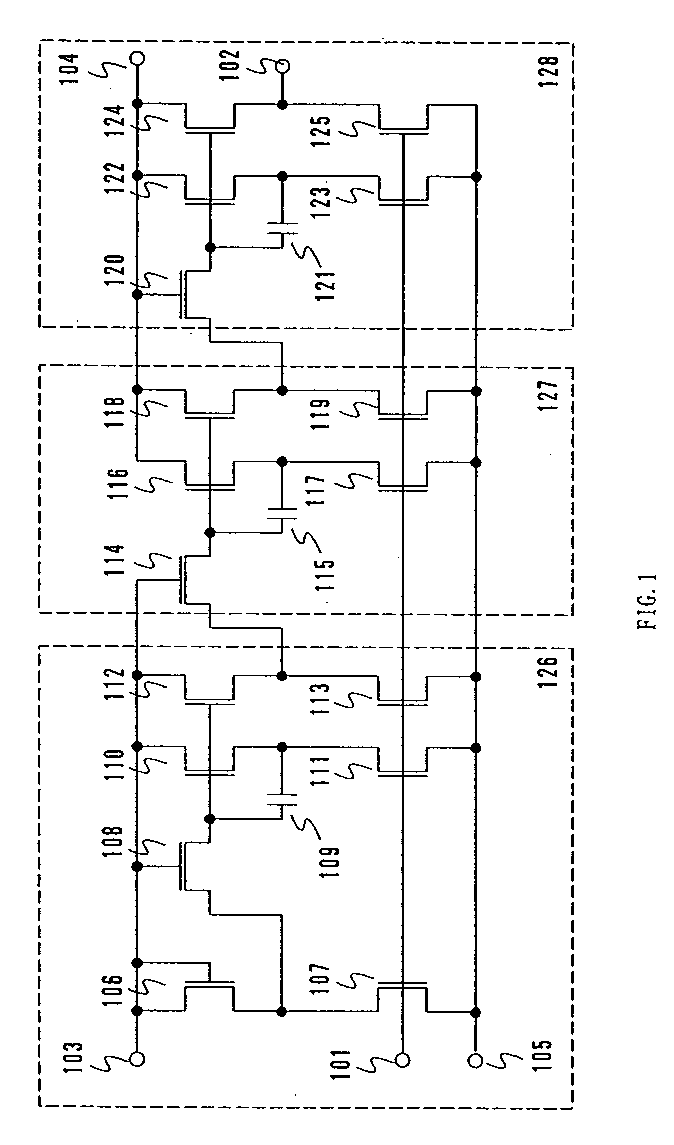
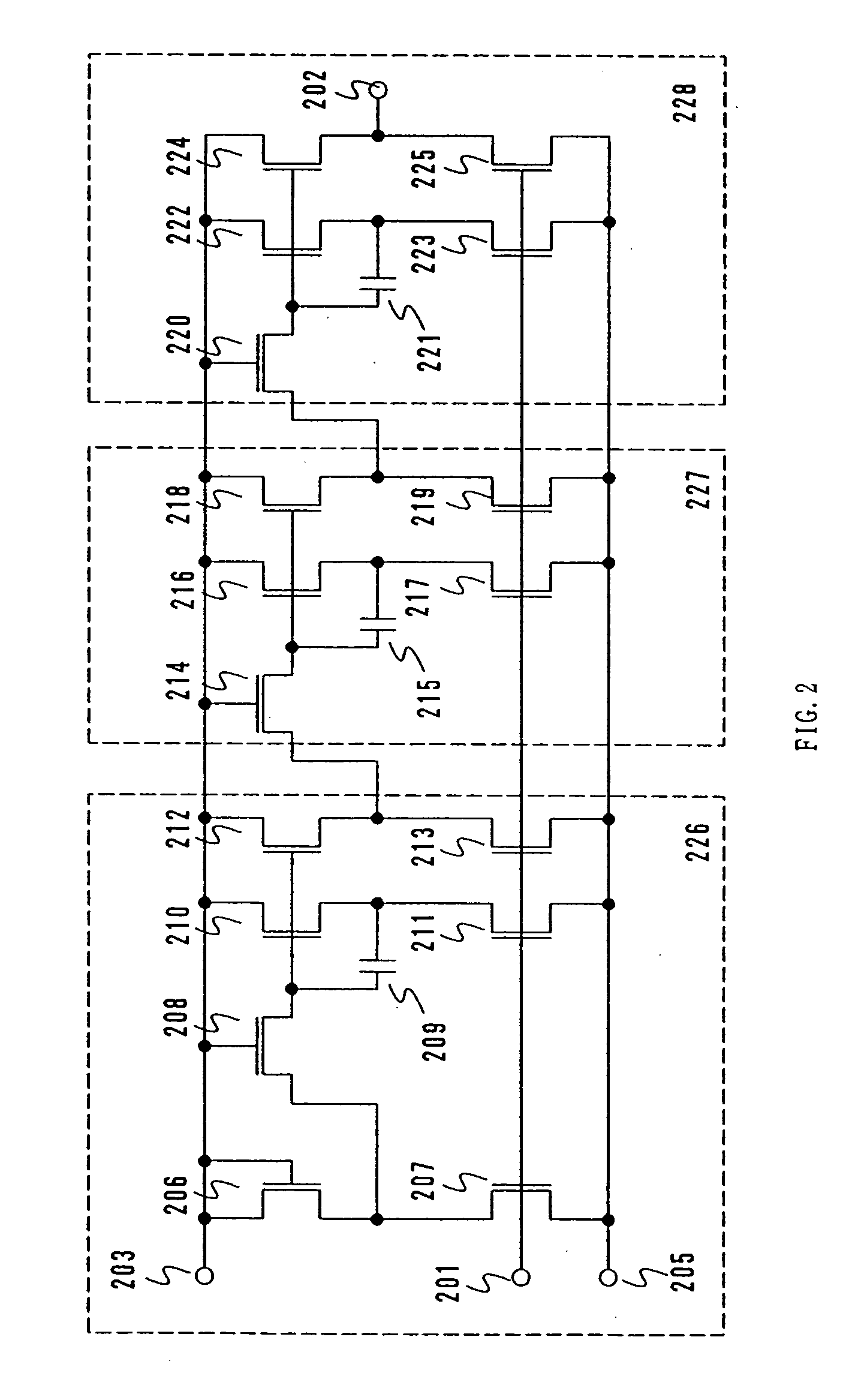
[0052]FIG. 5 is a block diagram showing a gate signal line driver circuit adopting the level shifter of the invention. As shown in FIG. 5, the gate signal line driver circuit comprises a shift register and a buffer circuit which includes a level shifter. The shift register is connected to a first power supply terminal and circuits for driving a gate signal line are connected to a second power supply terminal. A voltage of the first power supply terminal is set lower than that of the second power supply terminal, which prevents the reliability of the shift register from being lowered.

[0053]FIG. 6 shows a layout of the level shifter of the invention. A gate signal line is subjected to high loads, particularly in a display device having a large display area. Therefore, in FIG. 6, the last stage circuit for driving the gate signal line comprises a transistor whose gate is 400 μm in width in order to maintain the current capacity.

embodiment 2

[0054] Embodiment 2

[0055] Manufacturing steps of the display device of the invention are specifically explained hereinafter taking a liquid crystal display device as an example.

[0056] For a first substrate 10, a plastic material can be used as well as glass and quartz. Alternatively, an insulating layer may be formed on a metal material such as stainless and aluminum in order to obtain the first substrate 10. A first conductive layer 11 for forming a gate electrode and a gate wiring (scan line) is formed on the first substrate 10. For the first conductive layer 11, a metal material such as chrome, molybdenum, titanium, tantalum, tungsten, and aluminum, or an alloy of these materials is used. The first conductive layer 11 can be formed by sputtering or vacuum vapor deposition (FIG. 7A).

[0057] The first conductive layer 11 is etched to form gate electrodes 12 and 13. The gate electrodes 12 and 13 preferably have tapered ends so that a first semiconductor layer and a wiring layer are...

embodiment 3

[0083] Embodiment 3

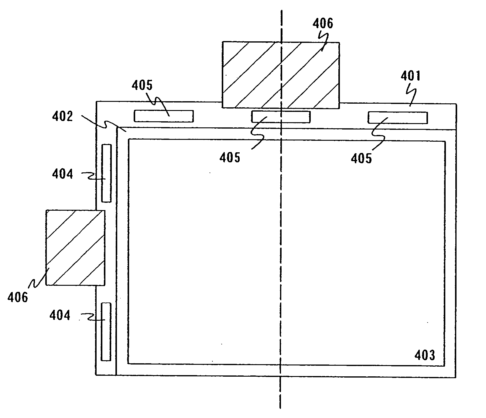
[0084]FIG. 11A is a plan view of a liquid crystal display device using the invention. The liquid crystal display device shown in FIG. 11A comprises a semi-amorphous TFT substrate 1101, a counter substrate 1102, a pixel portion 1103, a gate signal line driver circuit 1104, a source signal line driver circuit 1105, and an FPC 1106. FIG. 11B is a cross sectional view taken by cutting along a dotted line of the liquid crystal display device in FIG. 11A. A liquid crystal material is disposed between the semi-amorphous TFT substrate 1101 and the counter substrate 1102, and sealed with a sealing member 1107.

[0085] As set forth above, according to the invention, the gate signal line driver circuit 1104 is integrally formed on the substrate by using semi-amorphous TFTs, leading to reduction in the cost of implementation and improvement of the reliability in connecting parts. In FIG. 11A, the source signal line driver circuit 1105 is mounted on the semi-amorphous TFT subst...


PUM

PropertyMeasurementUnit
grain sizeaaaaaaaaaa
pressureaaaaaaaaaa
temperatureaaaaaaaaaa

Abstract

When semi-amorphous TFTs are used for forming a signal line driver circuit and a pixel, a large amplitude is required for driving the pixel, and a large power supply voltage is thus needed. On the other hand, when a shift register is made up of transistors having a single conductivity, a bootstrap circuit is required, and a voltage over a power supply is applied to a specific element. Therefore, not both the driving amplitude and the reliability can be achieved with a single power supply. According to the invention, a level shifter having a single conductivity is provided to solve such a problem.

Description

BACKGROUND OF THE INVENTION [0001] 1. Field of the Invention [0002] The present invention relates to a display device, and more particularly, to a display device comprising an element using a semi-amorphous thin film semiconductor. The invention further relates to an electronic apparatus using the display device. [0003] 2. Description of the Related Art [0004] In recent years, Internet has been widely used with the development of communication technologies. It is expected that moving pictures and larger amount of information are transmitted in the future. In view of this, personal computers have been popularized for private use and on business, and a large sized display device such as a liquid crystal television has also been produced in quantities and popularized. [0005] Among the display devices, a display device using a thin film transistor (hereinafter referred to as a TFT), such as a liquid crystal display device in particular, has been manufactured actively. An active matrix d...

Claims


Application Information

Patent Timeline
Patent Type & Authority Applications(United States)
IPC IPC(8): G02F1/133G02F1/1368G02F1/1362G09F9/00G09F9/30G09G3/20G09G3/30G09G3/36H01L21/77H01L21/84H01L27/12H01L29/04H01L29/786H01L51/50
CPCG02F1/13454G02F1/13624G09G3/20G09G2300/0408H01L29/78678G09G2310/0289H01L27/1214H01L29/04H01L29/78669G09G2300/08H01L27/1288
Inventor KOYAMA, JUNIMAI, KEITAROMAEKAWA, SHINJIFURUNO, MAKOTONAKAMURA, OSAMUYAMAZAKI, SHUNPEI
Owner SEMICON ENERGY LAB CO LTD
Why Eureka
Try Eureka