Field effect transistor and method for fabricating the same

a field effect transistor and transistor technology, applied in the field of field effect transistors, can solve the problems of reducing yield, disadvantageous cost of gate electrode forming procedure, and difficulty in realizing a device with high frequency characteristics equivalent or better, and achieves accurate control, low series resistance, and high reproducibility.

Active Publication Date: 2010-11-16
PANASONIC CORP
View PDF7 Cites 30 Cited by
  • Summary
  • Abstract
  • Description
  • Claims
  • Application Information

AI Technical Summary

Benefits of technology

[0015]In the first field effect transistor of this invention, the gate electrode can be formed by filling the opening with an electrode material. Accordingly, a short-gate length T-shaped gate electrode can be easily formed without performing electron-beam exposure. Also, since the insulating film is formed on the inner wall of the opening, the gate length can be made shorter than the width of a mask used for forming the opening. Furthermore, a gate leakage current can be reduced.
[0034]In the method for fabricating a field effect transistor of the invention, the width of the mask along the gate length direction is preferably smaller than a thickness thereof in the step (b), and the etching performed in the step (g) is preferably isotropic etching performed along directions of the width and the thickness. Thus, the line width of the mask layer can be easily reduced.

Problems solved by technology

Accordingly, it is difficult to realize a device with high frequency characteristics equivalent to or better than those of the GaAs-based or InP-based semiconductor unless a shorter gate length than in using a conventional compound semiconductor is realized.
Also, it is necessary to use the three-layered photoresist, and therefore, the cost of the procedure for forming the gate electrode is disadvantageously high.
Furthermore, reproducibility of the procedure for forming the T-shaped gate electrode is poor, and the gate electrode easily collapses, which disadvantageously lowers the yield.

Method used


Image

  • Field effect transistor and method for fabricating the same
  • Field effect transistor and method for fabricating the same
  • Field effect transistor and method for fabricating the same

Examples


embodiment 1

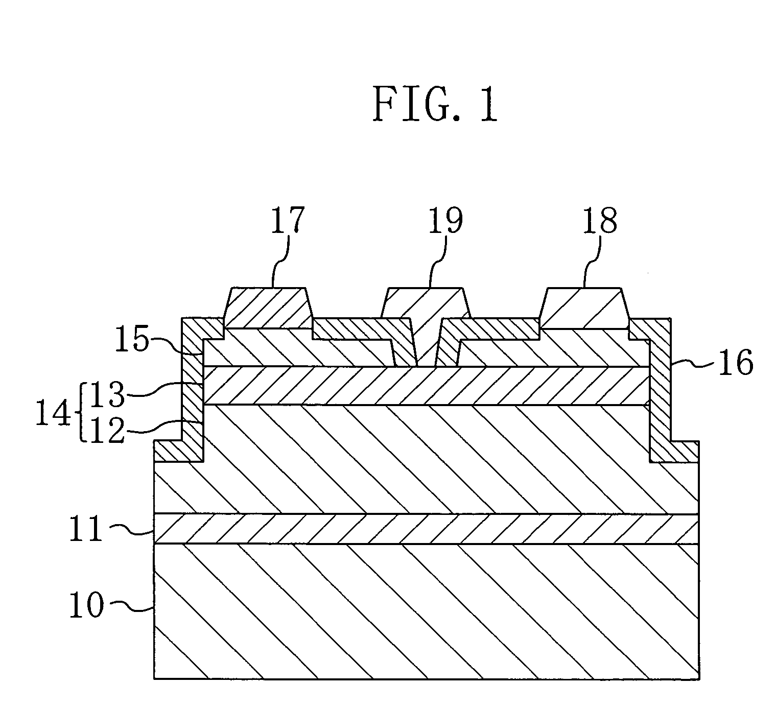
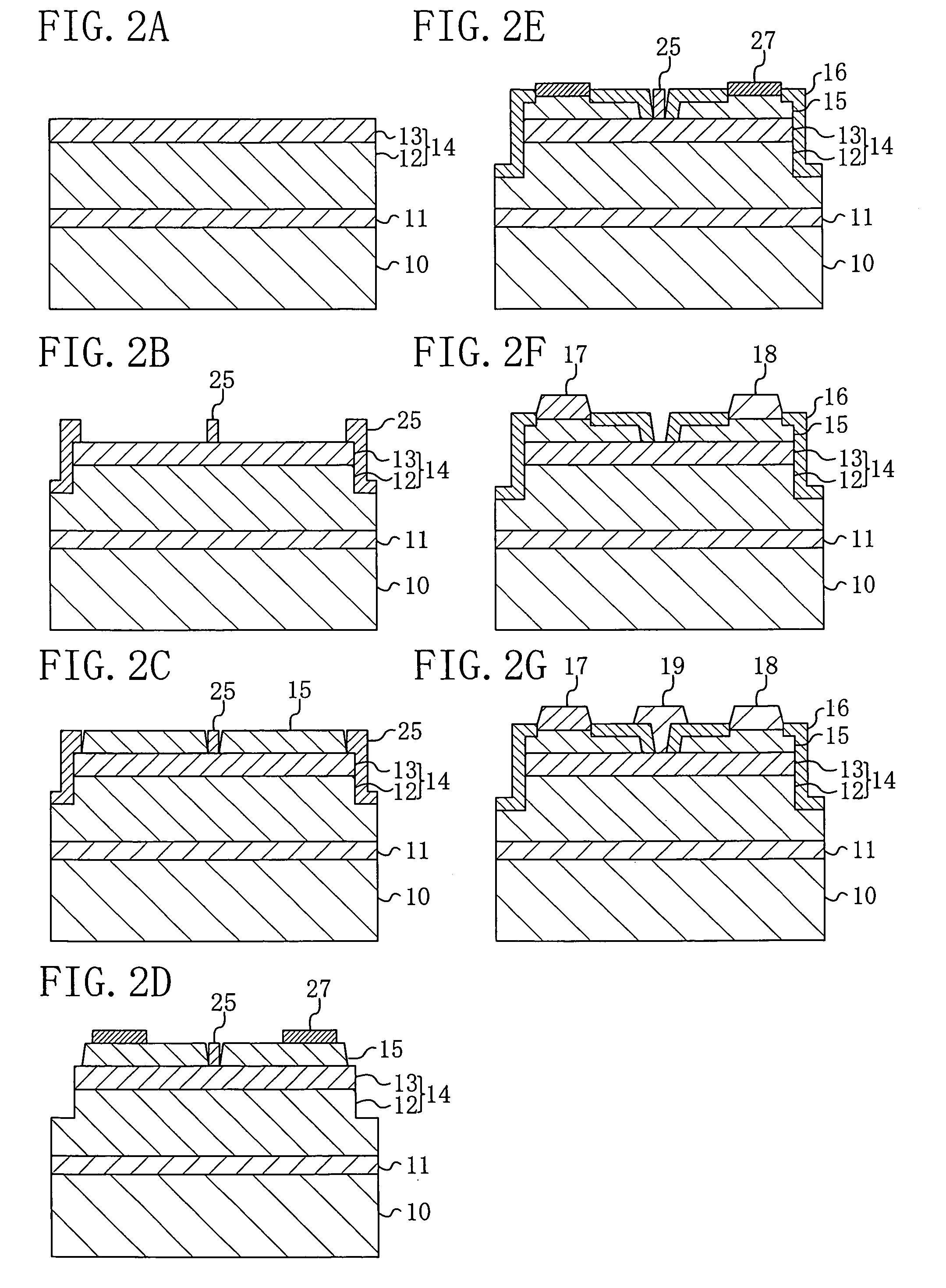
[0046]Embodiment 1 of the invention will now be described with reference to the accompanying drawings. FIG. 1 shows the cross-sectional structure of a field effect transistor (FET) according to Embodiment 1 of the invention. As shown in FIG. 1, a first semiconductor layer 14 composed of an undoped GaN film 12 and an n-type AlGaN film 13 successively stacked and a second semiconductor layer 15 made of n-type AlGaN are successively formed above a substrate 10 of sapphire with a buffer layer 11 of AlN disposed between the substrate 10 and the first semiconductor layer 14.

[0047]A source electrode 17 and a drain electrode 18 made of Ti, Al, Ni and Au successively stacked are formed on the second semiconductor layer 15 to be spaced from each other. In regions outside the source electrode 17 and the drain electrode 18, the second semiconductor layer 15, the AlGaN film 13 and part of the GaN film 12 of the first semiconductor layer 14 are selectively etched for isolation.

[0048]In a region o...

embodiment 2

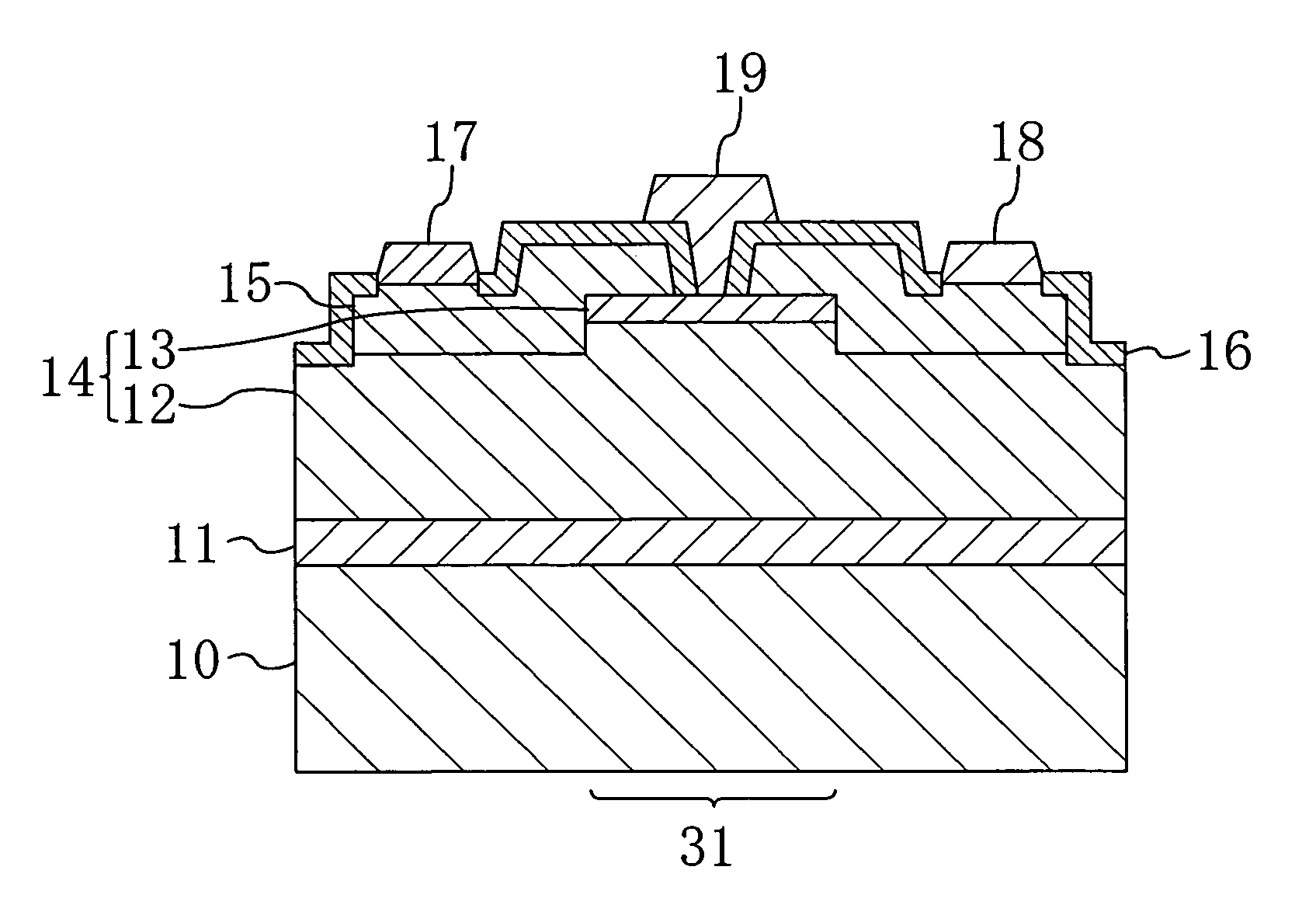
[0064]Embodiment 2 of the invention will now be described with reference to the accompanying drawings. FIG. 3 shows the cross-sectional structure of an FET according to Embodiment 2. In FIG. 3, like reference numerals are used to refer to like elements shown in FIG. 1 so as to omit the description.

[0065]As shown in FIG. 3, the FET of this embodiment is characterized by a mesa portion 31 formed in a first semiconductor layer 14. A buffer layer 11 of AlN is formed on a substrate 10 of GaN with a dislocation density as low as approximately 1×106 cm−2. An undoped GaN film 12 and an n-type AlGaN film 13 are successively deposited on the buffer layer 11, thereby forming the first semiconductor layer 14. The mesa portion 31 with a width of approximately 1 μm is formed in a part of the structure of the first semiconductor layer 14 made of the multilayer of the GaN film 12 and the AlGaN film 13. A second semiconductor layer 15 of n-type GaN is regrown so as to cover the top face and the side...

embodiment 3

Modification of Embodiment 3

[0095]A modification of Embodiment 3 will now be described with reference to the accompanying drawing. FIG. 8 shows the cross-sectional structure of a semiconductor device according to a modification of Embodiment 3. In FIG. 8, like reference numerals are used to refer to like elements shown in FIG. 5 so as to omit the description.

[0096]As shown in FIG. 8, in the semiconductor device of this modification, a first semiconductor layer 14 and a second semiconductor layer 15 are formed on an R-plane corresponding to the (1-102) plane of the plane direction of a substrate 40 of sapphire. The principal plane of the first semiconductor layer 14 and the second semiconductor layer 15 formed on the R-plane of the substrate 40 is an A-plane corresponding to the (11-20) plane of the plane direction. Since polarization is not caused vertically to the A-plane, no carriers are generated on an undoped hetero interface. Also, since an AlN film 63 has a very large band gap...


PUM


Abstract

A field effect transistor includes a first semiconductor layer made of a multilayer of a plurality of semiconductor films and a second semiconductor layer formed on the first semiconductor layer. A source electrode and a drain electrode are formed on the second semiconductor layer to be spaced from each other. An opening having an insulating film on its inner wall is formed in a portion of the second semiconductor layer sandwiched between the source electrode and the drain electrode so as to expose the first semiconductor layer therein. A gate electrode is formed in the opening to be in contact with the insulating film and the first semiconductor layer on the bottom of the opening.

Description

CROSS-REFERENCE TO RELATED APPLICATIONS[0001]This application claims priority under 35 U.S.C. §119 on Patent Application No. 2004-356369 filed in Japan on Dec. 9, 2004, the entire contents of which are hereby incorporated by reference. The entire contents of Patent Application No. 2005-348790 filed in Japan on Dec. 2, 2005 are also incorporated by reference.BACKGROUND OF THE INVENTION[0002]The present invention relates to a field effect transistor and a method for fabricating the same, and more particularly, it relates to a high-power transistor, a high-frequency transistor or the like using a nitride semiconductor and a method for fabricating the same.[0003]A group III-V nitride compound semiconductor typified by gallium nitride (GaN) or the like, namely, what is called a nitride semiconductor, is a wide gap semiconductor, and the band gap at room temperature of, for example, gallium nitride (GaN) is 3.4 eV and that of aluminum nitride (AlN) is 6.2 eV. A nitride semiconductor is ch...

Claims


Application Information

Patent Timeline
Patent Type & Authority Patents(United States)
IPC IPC(8): H01L29/66
CPCH01L21/28581H01L29/66462H01L29/7787H01L29/2003H01L29/0843
Inventor UEDA, TETSUZOISHIDA, HIDETOSHITANAKA, TSUYOSHI
Owner PANASONIC CORP
Why Eureka
Try Eureka