Photomask

a technology of photomasks and masks, applied in the field of photomasks, can solve the problems of difficult to increase the process margin in the exposure using a photomask, and achieve the effect of improving the contrast in the light intensity distribution and increasing the process margin

Inactive Publication Date: 2010-11-30
PANASONIC CORP
View PDF12 Cites 3 Cited by
  • Summary
  • Abstract
  • Description
  • Claims
  • Application Information

AI Technical Summary

Benefits of technology

[0017]Therefore, the present inventor has variously examined a mask architecture capable of increasing a process margin even when a pattern to be applied for the mask enhancer structure is close to another pattern. As a result, it has been found that a process margin can be increased even in complicated patterns mixedly having arbitrary pattern layouts by employing a mask architecture in which the width of a phase shifter included in the mask enhancer structure of the pattern is made smaller as a distance from another close pattern is smaller.
[0047]As described so far, according to the present invention, the effects to improve contrast in a light intensity distribution and to increase a process margin can be sufficiently attained by employing the mask enhancer structure also in a photomask including not only an isolated pattern but also complicated patterns close to one another. Also, since the width of the phase shifter of the mask enhancer structure can be optimized in accordance with the close relationship between patterns or the shielding property of an adjacent pattern, a photomask capable of fine pattern formation with random pattern layout can be realized.

Problems solved by technology

Accordingly, it is difficult to increase a process margin in exposure using a photomask having complicated patterns mixedly having arbitrary pattern layouts simply by determining the architecture of the pattern having the mask enhancer structure on the basis of the line width of the pattern.

Method used


Image

  • Photomask
  • Photomask
  • Photomask

Examples


embodiment 1

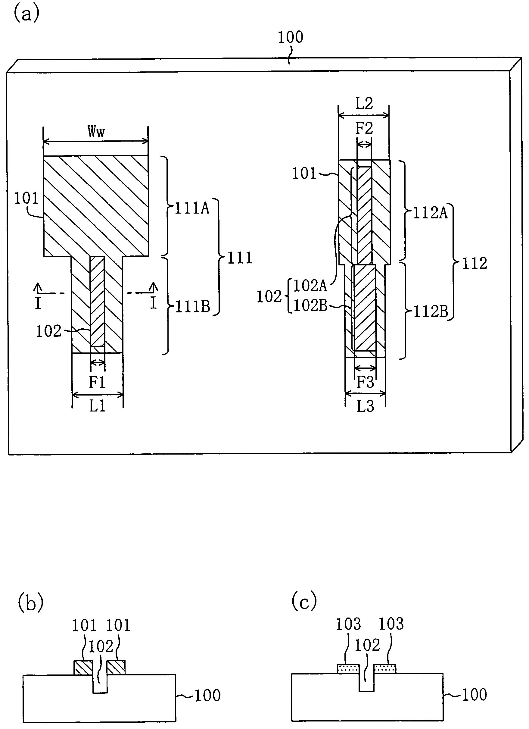
[0092]A photomask according to Embodiment 1 of the invention will now be described with reference to the accompanying drawings.

[0093]FIG. 3A is a plan view of the photomask of Embodiment 1 and FIG. 3B is a cross-sectional view taken on line II-II of FIG. 3A. It is noted that a transparent substrate 100 is perspectively shown in FIG. 3A.

[0094]As shown in FIG. 3A, mask patterns (line patterns 121 through 123) used for forming desired line-shaped patterns on a wafer through exposure are drawn on the transparent substrate 100. At this point, each of the line patterns 121 through 123 is basically made of a shielding portion 101. Also, in a central portion of a pattern region with a line width not larger than a given dimension W0 in each of the line patterns 121 through 123, the shielding portion 101 has an opening in which a phase shifter 102 is provided. In other words, each of the line patterns 121 through 123 has the mask enhancer structure. For example, the pattern 121 is a pattern w...

modification 1

of Embodiment 1

[0134]A photomask according to Modification 1 of Embodiment 1 of the invention will now be described with reference to the accompanying drawings.

[0135]FIG. 11 is a plan view of the photomask of Modification 1 of Embodiment 1, and more specifically, a photomask provided with a mask pattern having the mask enhancer structure and included in densely arranged patterns. In FIG. 11, a transparent substrate 100 is perspectively shown.

[0136]As shown in FIG. 11, mask patterns (line patterns 124 through 128) for forming desired line-shaped patterns on a wafer through exposure are drawn on the transparent substrate 100. In this case, each of the line patterns 124 through 128 is basically made of a shielding portion 101. Furthermore, a phase shifter 102 is provided at the center of a pattern region of each of the line patterns 124 through 128 having a line width not larger than a given dimension WO. Specifically, each of the line patterns 124 through 128 has the mask enhancer str...

modification 2

of Embodiment 1

[0155]A photomask according to Modification 2 of Embodiment 1 of the invention will now be described with reference to the accompanying drawings.

[0156]FIG. 14 is a plan view of the photomask of Modification 2 of Embodiment 1, and more specifically, a photomask provided with a mask pattern having the mask enhancer structure and included in densely arranged patterns. In FIG. 14, a transparent substrate 100 is perspectively shown.

[0157]As shown in FIG. 14, mask patterns (line patterns 131 through 135) for forming desired line-shaped patterns on a wafer through exposure are drawn on the transparent substrate 100. In this case, each of the line patterns 131 through 135 is basically made of a shielding portion 101. Furthermore, a phase shifter 102 is provided at the center of a pattern region, having a line width not larger than a given dimension WO, of each of the line patterns 131 through 133. Specifically, each of the line patterns 131 through 133 has the mask enhancer s...


PUM

PropertyMeasurementUnit
thicknessaaaaaaaaaa
transmittanceaaaaaaaaaa

Abstract

A pattern 121 provided on a transparent substrate 100 as a mask pattern includes partial patterns 121A and 121B. Each of the partial patterns 121A and 121B has a mask enhancer structure including a phase shifter 102 for transmitting exposing light in an opposite phase with respect to a transparent portion and a shielding portion 101 surrounding the phase shifter 102. The partial pattern 121A is close to other patterns 122 and 123 at distances not larger than a given distance with the transparent portion sandwiched therebetween. The width of the phase shifter 102A of the partial pattern 121A is smaller than the width of the phase shifter 102B of the partial pattern 121B.

Description

[0001]This application is the U.S. National Phase under 35 U.S.C. §371 of International Application No. PCT / JP2004 / 014143, filed Sep. 21, 2004, which in turn claims the benefit of Japanese Application No. 2003-362717, filed Oct. 23, 2003, the disclosures of which Applications are incorporated by reference herein in their entirety.TECHNICAL FIELD[0002]The present invention relates to a photomask for use in forming a fine pattern in fabrication of a semiconductor integrated circuit device or the like and a design method for the same.BACKGROUND ART[0003]Recently, there are increasing demands for further refinement of circuit patterns for increasing the degree of integration of a large scale integrated circuit device (hereinafter referred to as the LSI) realized by using semiconductor. As a result, it has become very significant to thin an interconnect pattern included in a circuit.[0004]Now, the thinning of an interconnect pattern by a conventional optical exposure system will be descr...

Claims


Application Information

Patent Timeline
Patent Type & Authority Patents(United States)
IPC IPC(8): G03F1/00G03F1/29G03F1/36G03F1/68G03F7/20G06F17/50H01L21/027
CPCG03F1/144G03F1/30G03F1/36
Inventor MISAKA, AKIO
Owner PANASONIC CORP
Why Eureka
Try Eureka