

Organic EL emission devices connected in series
a technology of organic el and emission devices, applied in the direction of discharge tube luminescnet screens, discharge tube/lamp details, luminescent compositions, etc., can solve problems such as heat generation, interconnection section deterioration, and (ii) are not solved, and achieve excellent whiteness uniformity
- Summary
- Abstract
- Description
- Claims
- Application Information
AI Technical Summary
Benefits of technology
Problems solved by technology
Method used
Image

Examples
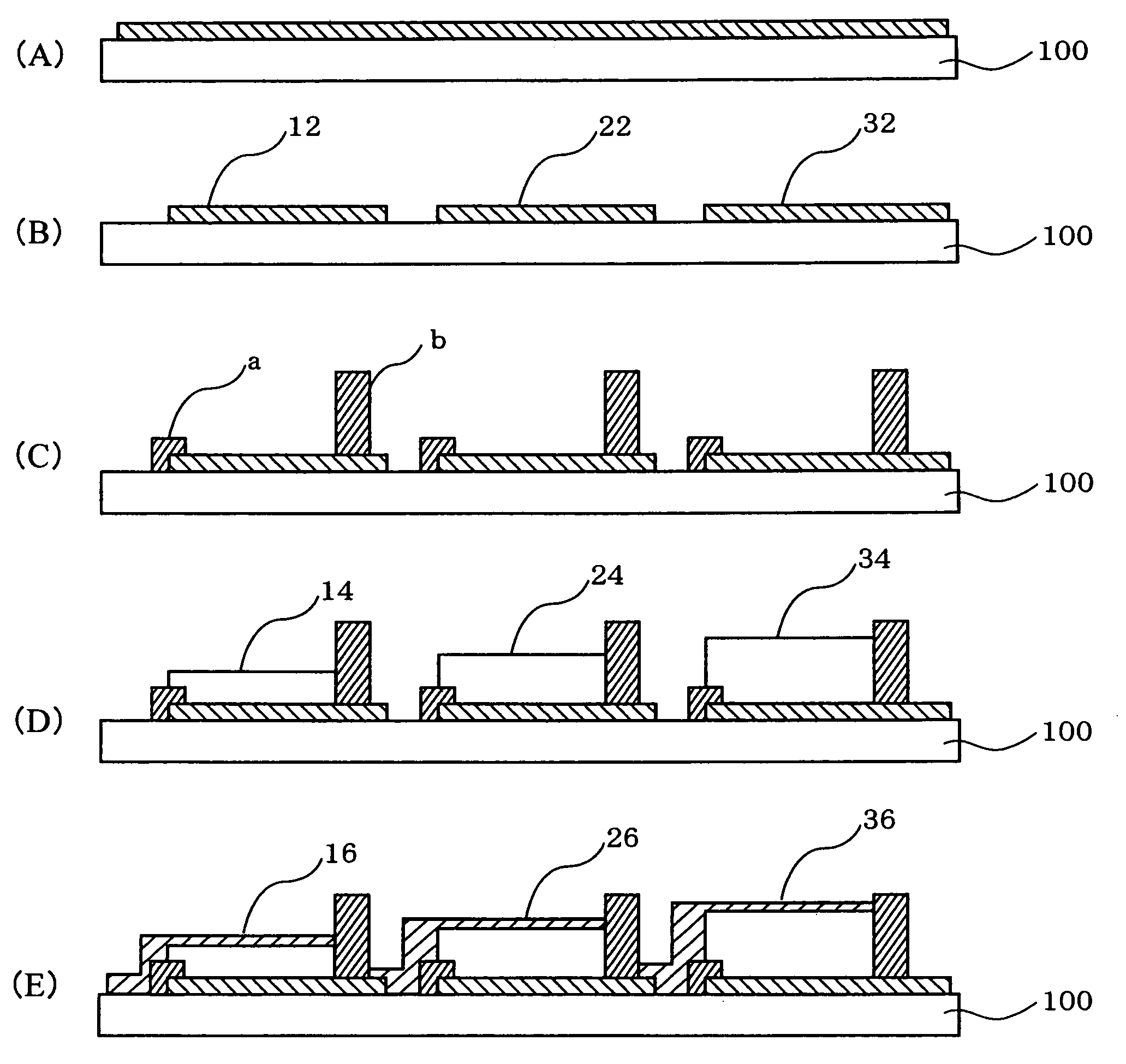
first embodiment
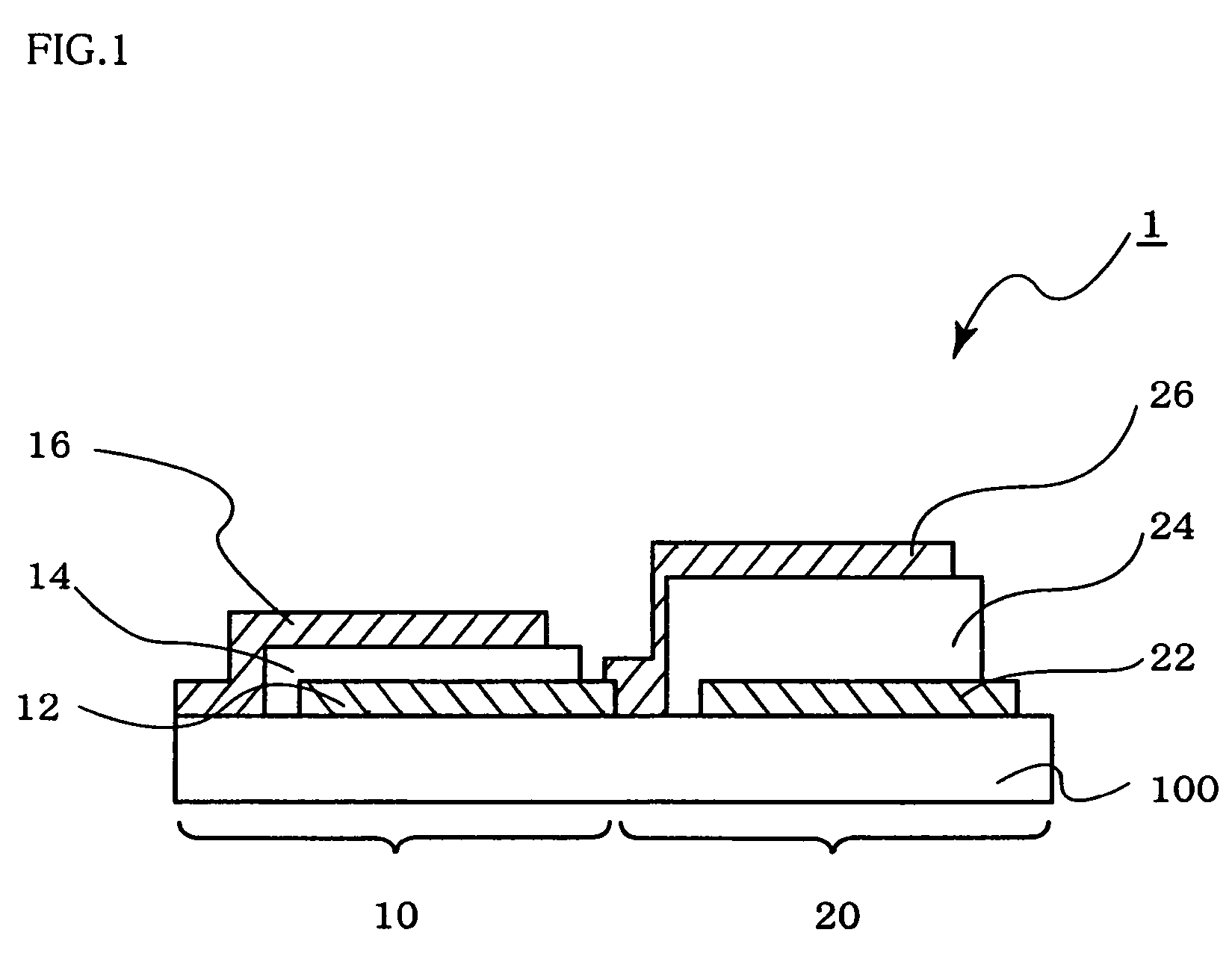
1. First Embodiment
[0035]FIG. 1 schematically illustrates a first embodiment of the invention.
[0036]As illustrated in this view, an organic EL apparatus 1 has a first emitting device 10 and a second emitting device 20 arranged in parallel on a substrate 100.
[0037]The first emitting device 10 has a structure wherein a first under, or lower, electrode 12, a first organic emitting layer 14, and a first upper electrode 16 are stacked, in this order, on the substrate 100.
[0038]The second emitting device 20 has a structure wherein a second under, or lower, electrode 22, a second organic emitting layer 24, and a second upper electrode 26 are stacked, in this order, on the substrate 100.
[0039]The first and second under, or lower, electrodes 12 and 22 each functions as an anode for injecting holes into the organic emitting layer or a cathode for injecting electrons into the organic emitting layer. When the first under, or lower, electrode 12 is the cathode, the second upper electrode 26 is t...
second embodiment
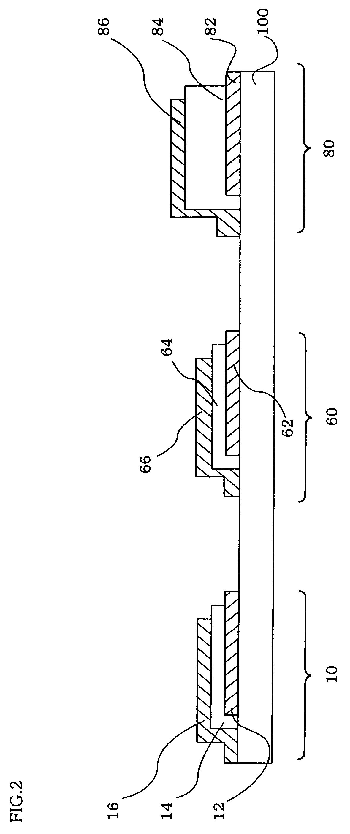
2. Second Embodiment
[0062]FIG. 8 is a schematic view illustrating a second embodiment of the invention.
[0063]As illustrated in this view, an organic EL apparatus 2 is different from the first embodiment only in that the apparatus has a third emitting device 30. In other words, the organic EL emitting device 2 has a first emitting device 10, a second emitting device 20 and a third emitting device 30 arranged on a substrate 100. The first emitting device 10 and the second emitting device 20 are the same as in the above-mentioned first embodiment. Thus, description thereof is not repeated here.
[0064]The third emitting device 30 has a structure wherein a third under electrode 32, a third organic emitting layer 34 and a third upper electrode 36 are stacked, in this order, on substrate 100. The second under electrode 22 and the third upper electrode 36 are electrically connected to each other. The second under electrode 22 and the third upper electrode 36 may be made of the same material ...
third embodiment
3. Third Embodiment
[0072]FIG. 12 illustrates a third embodiment of the invention.
[0073]As illustrated in this view, the third embodiment has a structure wherein a light diffusible member 40 is provided in the organic EL apparatus of the second embodiment and is present on the light emission side relative to the upper electrodes of the emitting devices thereof.
[0074]FIG. 13 is a chart illustrating a radiation pattern representing the angle dependency of the emission intensity of the above-mentioned organic EL apparatus wherein its emission medium layer is made of Alq3. The radiation patterns of the cases where the NPD thickness is 60 nm and 205 nm are represented by B and C, respectively, and the radiation pattern of the case where a single reflective layer is present is represented by A′. As understood from FIG. 13, in the structure wherein the two reflection surfaces are arranged and further the FWHM of the EL spectrum is made more narrow than the natural emission bandwidth of the ...
PUM
 Abstract
Description
Claims
Application Information