
Light source device and image display apparatus

Inactive Publication Date: 2010-12-14
SEIKO EPSON CORP
View PDF10 Cites 0 Cited by
  • Summary
  • Abstract
  • Description
  • Claims
  • Application Information

AI Technical Summary

Benefits of technology

[0011]According to such an arrangement, the use of the first optical element obviates the necessity of the long and thick convex portion or the L-shaped member for supporting the external resonator or the wavelength converting element. Moreover, the light emitting unit, the optical elements, and the external resonator are disposed and fixed to a base plate from the same direction, providing good workability at the time of manufacturing while decreasing manufacturing cycle time. In addition, the use of the second and third optical elements enables extraction of the harmonic laser beams returning back to the light emitting unit after being converted by the wavelength converting element in a more efficient manner than the case in which the harmonic laser beams are allowed to be reflected from the surface of the light emitting element. Accordingly, it is possible to simplify the configuration of the light source device while decreasing the manufacturing cost. Also, the device can have a low profile and high efficiency.Application Example 2
[0015]According to such an arrangement, the polarization direction of the fundamental laser beams can be arranged. Accordingly, it is possible to increase light utilization efficiency when the light source device is used in combination with devices such as liquid crystals in which polarization is controlled.Application Example 4
[0019]According to such an arrangement, it becomes easy to change the propagation direction of laser beams in an efficient manner and at low cost.Application Example 6
[0023]According to such an arrangement, it becomes easy to change the propagation direction of laser beams in an efficient manner and at low cost.Application Example 8
[0029]According to such an arrangement, the use of the first optical element obviates the necessity of the long and thick convex portion or the L-shaped member for supporting the external resonator or the wavelength converting element. Moreover, the light emitting unit, the optical elements, and the external resonator are disposed and fixed to a base plate from the same direction, providing good workability at the time of manufacturing while decreasing manufacturing cycle time. In addition, the use of the second and third optical elements enables extraction of the harmonic laser beams returning back to the light emitting unit after being converted by the wavelength converting element in a more efficient manner without needing to pass the harmonic laser beams through the wavelength converting element and the external resonator. Accordingly, it is possible to simplify the configuration of the image display apparatus while decreasing the manufacturing cost. Also, the apparatus can have a low profile and high efficiency.Application Example 11
[0031]According to such an arrangement, the use of the first optical element obviates the necessity of the long and thick convex portion or the L-shaped member for supporting the external resonator or the wavelength converting element. Moreover, the light emitting unit, the optical elements, and the external resonator are disposed and fixed to a base plate from the same direction, providing good workability at the time of manufacturing while decreasing manufacturing cycle time. In addition, the use of the second and third optical elements enables extraction of the harmonic laser beams returning back to the light emitting unit after being converted by the wavelength converting element in a more efficient manner without needing to pass the harmonic laser beams through the wavelength converting element and the external resonator. Accordingly, it is possible to simplify the configuration of the image display apparatus while decreasing the manufacturing cost. Also, the apparatus can have a low profile and high efficiency.

Problems solved by technology

On the other hand, the metal member having a long and thick protruding portion or the L-shaped metal member is manufactured by die-case methods or MIM (metal injection molding) methods, which may increase the manufacturing cost.
In addition, in the case of realizing the state by using a combination of two separate bodies, a process of bonding the two separate bodies into one body is required, thus complicating the manufacturing works and further increasing the cost.
Besides, a large space is required for preparation of such a long and thick convex portion or of the L-shaped member, and it is thus difficult to realize a sufficiently small size (low profile).
Also, the device can have a low profile and high efficiency.
Also, the apparatus can have a low profile and high efficiency.

Method used


Image

  • Light source device and image display apparatus
  • Light source device and image display apparatus
  • Light source device and image display apparatus

Examples


first embodiment

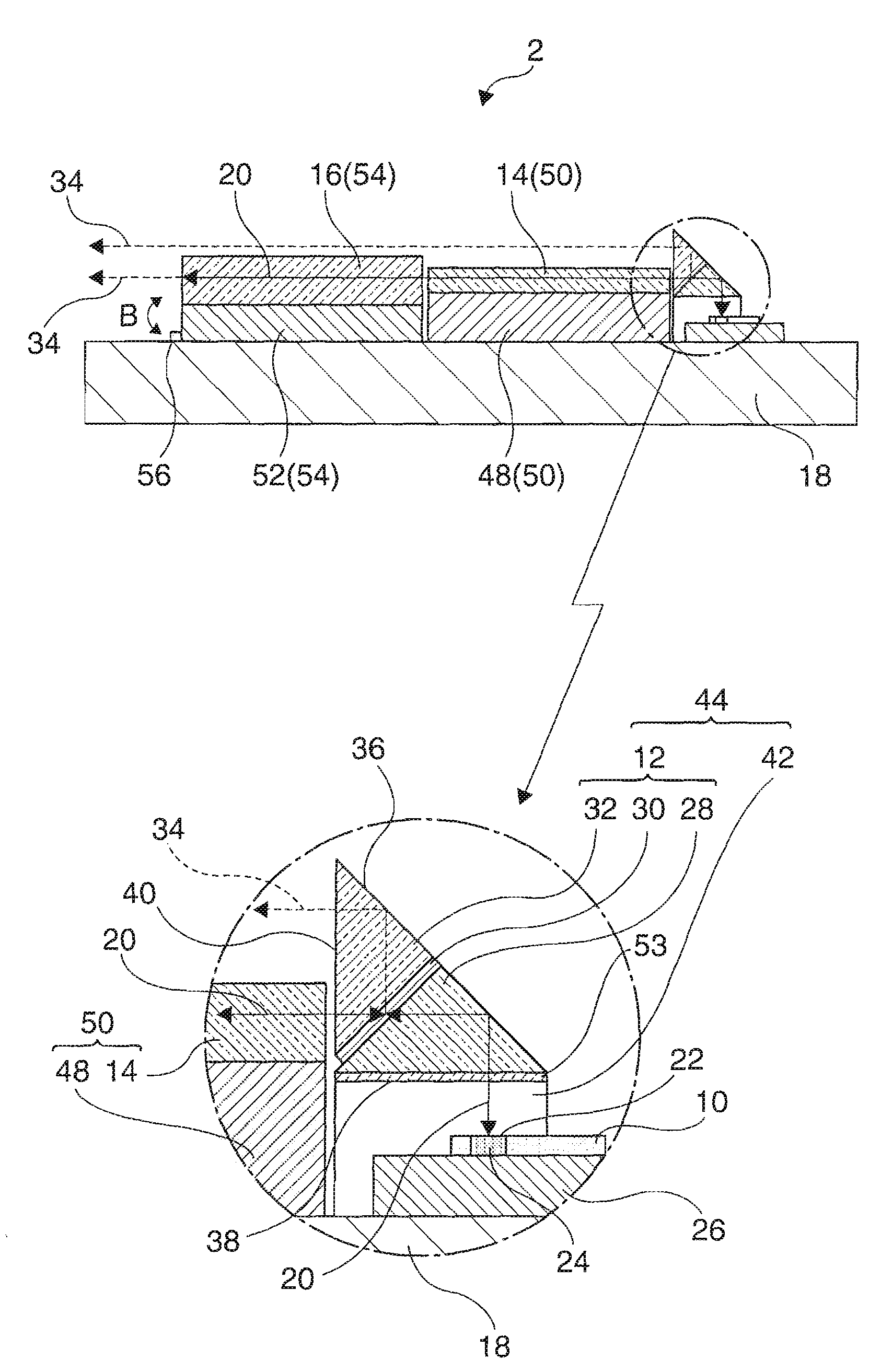
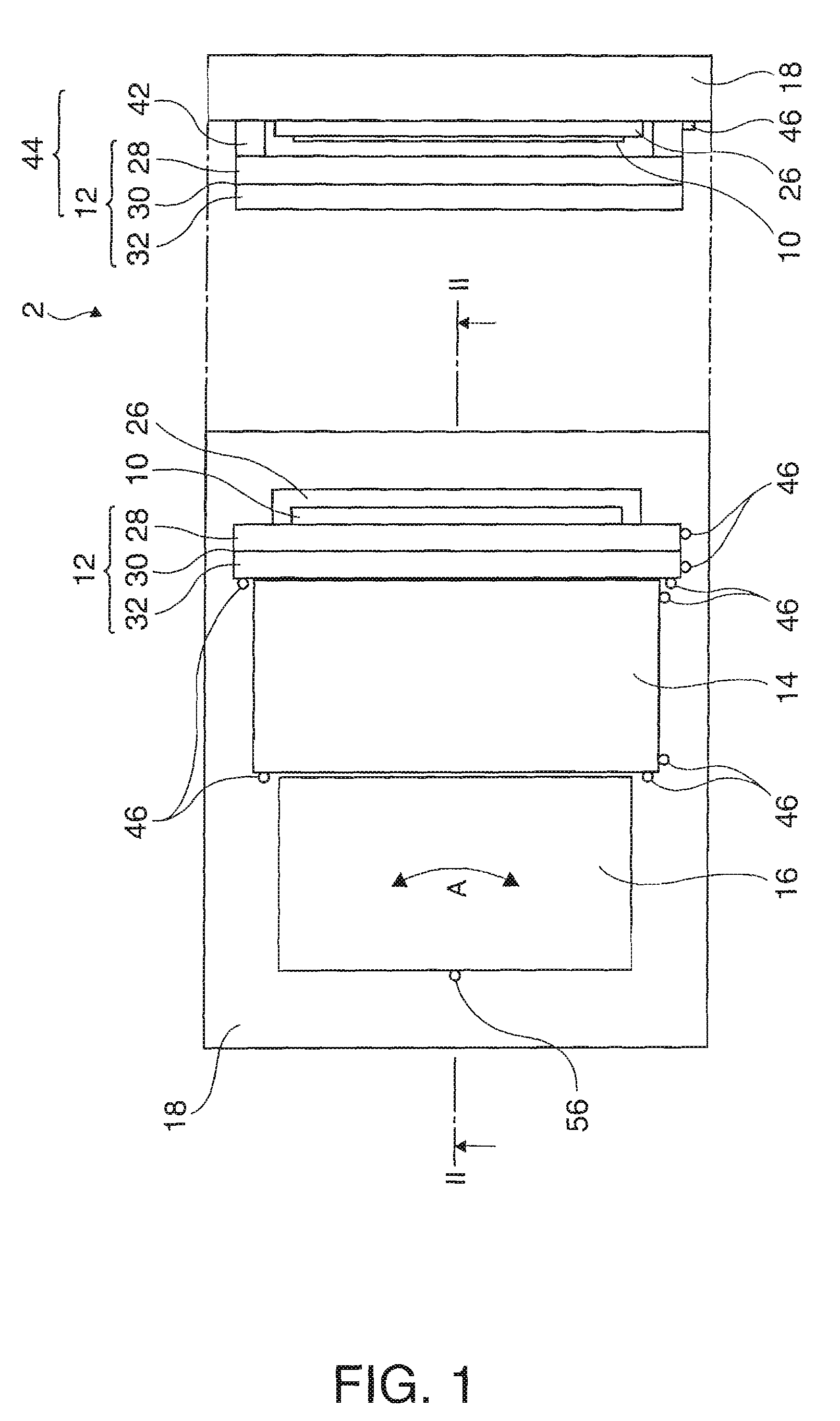
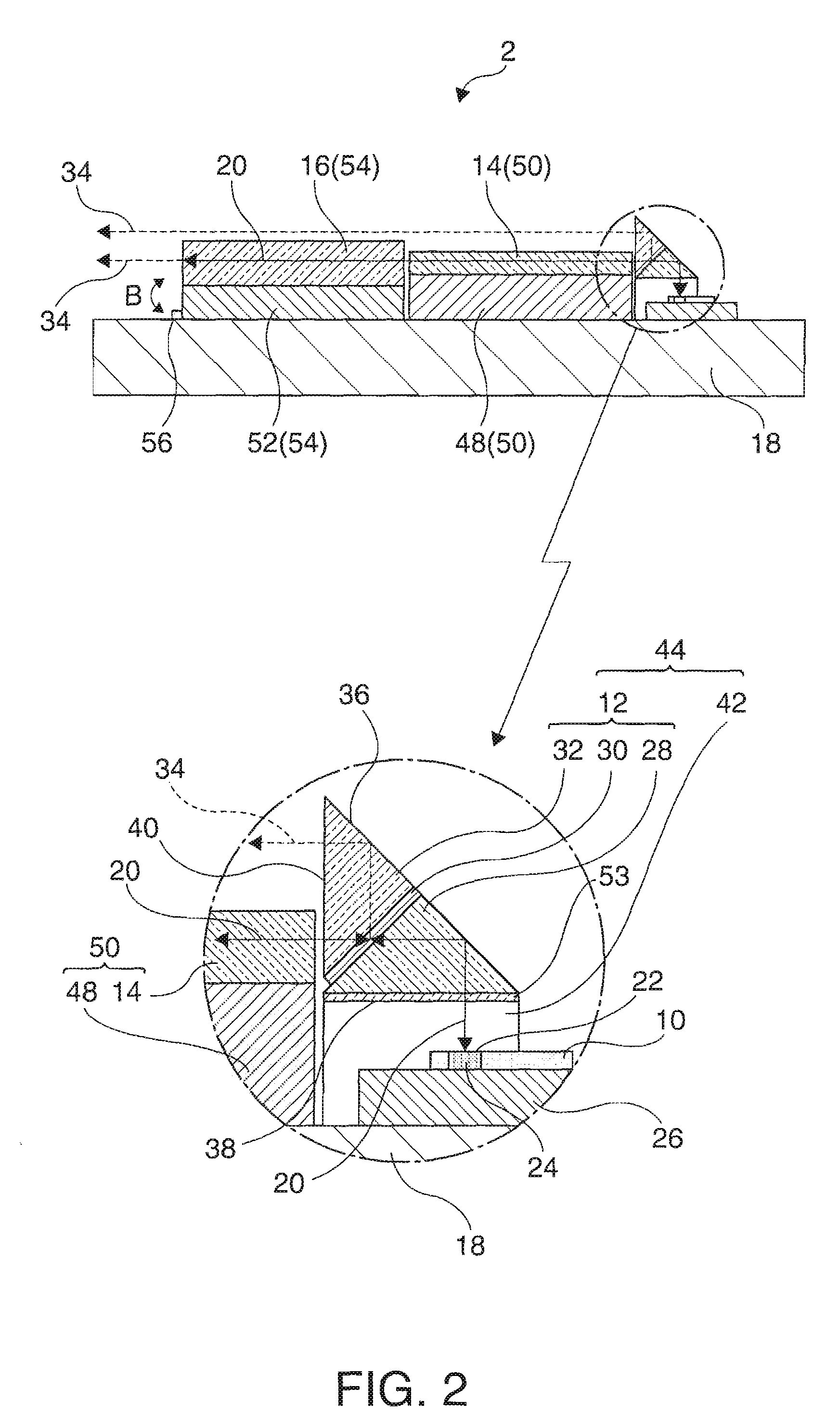
[0045]FIG. 1 shows a plan view and a side view of a light source device in accordance with a first embodiment. FIG. 2 shows a sectional view taken along the line II-II of FIG. 1. As shown in FIG. 1, the light source device 2 of the present embodiment includes a light emitting unit 10, an optical element 12, a wavelength converting element 14, an external resonator 16, and a base plate 18.

[0046]The light emitting unit 10 is supported by a support member 26, as shown in FIG. 2. The light emitting unit 10 includes one or more light emitting element (surface emission type semiconductor laser) 24 that emits fundamental laser beams 20 in a direction vertical to a light emitting surface 22. The light emitting unit 10 emits one or a plurality of fundamental laser beams 20. Semiconductor lasers, solid-state lasers, or the like are usable as the light emitting element 24.

[0047]The optical element 12 is disposed on an optical path of the fundamental laser beams 20 that are emitted by the light...

second embodiment

[0072]FIG. 4 shows a sectional view of a light source device in accordance with a second embodiment. FIG. 5 shows a sectional view taken along the line IV-IV of FIG. 4. FIG. 6 shows a sectional view taken along the line V-V of FIG. 4. Incidentally, identical reference numeral will be attached to components identical with or similar to the first embodiment, and description thereof will be omitted. As shown in FIG. 4, the light source device 4 of the present embodiment includes a light emitting unit 10, an optical element 58, a wavelength converting element 14, an external resonator 16, and a base plate 18.

[0073]The optical element 58 includes a first prism 60 as a first optical element, a wavelength separating film 30 as a second optical element, and a second prism 62 as a third optical element.

[0074]The first prism 60 deflects a propagation direction of the fundamental laser beams 20 that are emitted from the light emitting unit 10 having one or more light emitting element 24 emitti...

third embodiment

[0084]FIG. 7 shows a sectional view of a light source device in accordance with a third embodiment. Incidentally, identical reference numeral will be attached to components identical with or similar to the second embodiment, and description thereof will be omitted. As shown in FIG. 7, the light source device 6 of the present embodiment includes a light emitting unit 10, an optical element 74, a wavelength converting element 14, an external resonator 16, and a base plate 18.

[0085]The optical element 74 includes a first reflecting mirror (mirror) 76 as a first optical element, a wavelength separating film 30 as a second optical element, and a second reflecting mirror (mirror) 78 as a third optical element.

[0086]The first reflecting mirror 76 changes the propagation direction of the fundamental laser beams 20 emitted from the light emitting unit 10 and the harmonic laser beams 34 converted by the wavelength converting element 14. The first reflecting mirror 76 functions as an optical p...


PUM


Abstract

There are provided a light source device and an image display apparatus. The light source device includes a first optical element that deflects a propagation direction of laser beams, a second optical element that separates laser beams, and a third optical element that defects the laser beams separated by the second optical element. The light source device further includes a light emitting unit that has one or more light emitting element emitting laser beams, an external resonator that reflects laser beams toward the first optical element and guides laser beams back to the light emitting unit, and a wavelength converting element that converts laser beams.

Description

CROSS-REFERENCE TO RELATED APPLICATION[0001]This application claims priority from Japanese Patent Application No. 2006-318114 filed in the Japanese Patent Office on Nov. 27, 2006, and Japanese Patent Application No. 2007-175879 filed in the Japanese Patent Office on Jul. 4, 2007 the entire disclosures of which are hereby incorporated by reference in their entirety.BACKGROUND[0002]1. Technical Field[0003]Embodiments of the present invention relate to a light source device and an image display apparatus.[0004]2. Related Art[0005]Recently, in the field of opto-electronics, such as optical communication, optics-applied measurement or optical display, laser light source devices are widely used in which a semiconductor laser light source uses wavelength-converted oscillating light. As an example of such laser light source devices, Japanese Patent Application 2006-511966 (Patent Document 1) suggested an external resonance type laser to realize stable supply of laser beams having a narrow w...

Claims


Application Information

Patent Timeline
IPC IPC(8): H01S3/10
CPCG02B27/104G02B27/1046G02B27/141G02B27/149G03B21/28H01S5/14H01S3/109H01S5/005H01S5/0071H01S5/4087
Inventor TAKAGI, KUNIHIKOEGAWA, AKIRA
Owner SEIKO EPSON CORP
Features
  • Generate Ideas
  • Intellectual Property
  • Life Sciences
  • Materials
  • Tech Scout
  • Unparalleled Data Quality
  • Higher Quality Content
  • 60% Fewer Hallucinations
Learn More