
Method for making a multiple-wavelength opto-electronic device including a superlattice

a technology of optoelectronic devices and superlattices, applied in the field of semiconductor devices, can solve the problems of relative inefficiency and inpracticality, and achieve the effect of improving mobility characteristics

Active Publication Date: 2011-01-04
ATOMERA INC
View PDF71 Cites 86 Cited by
  • Summary
  • Abstract
  • Description
  • Claims
  • Application Information

AI Technical Summary

Benefits of technology

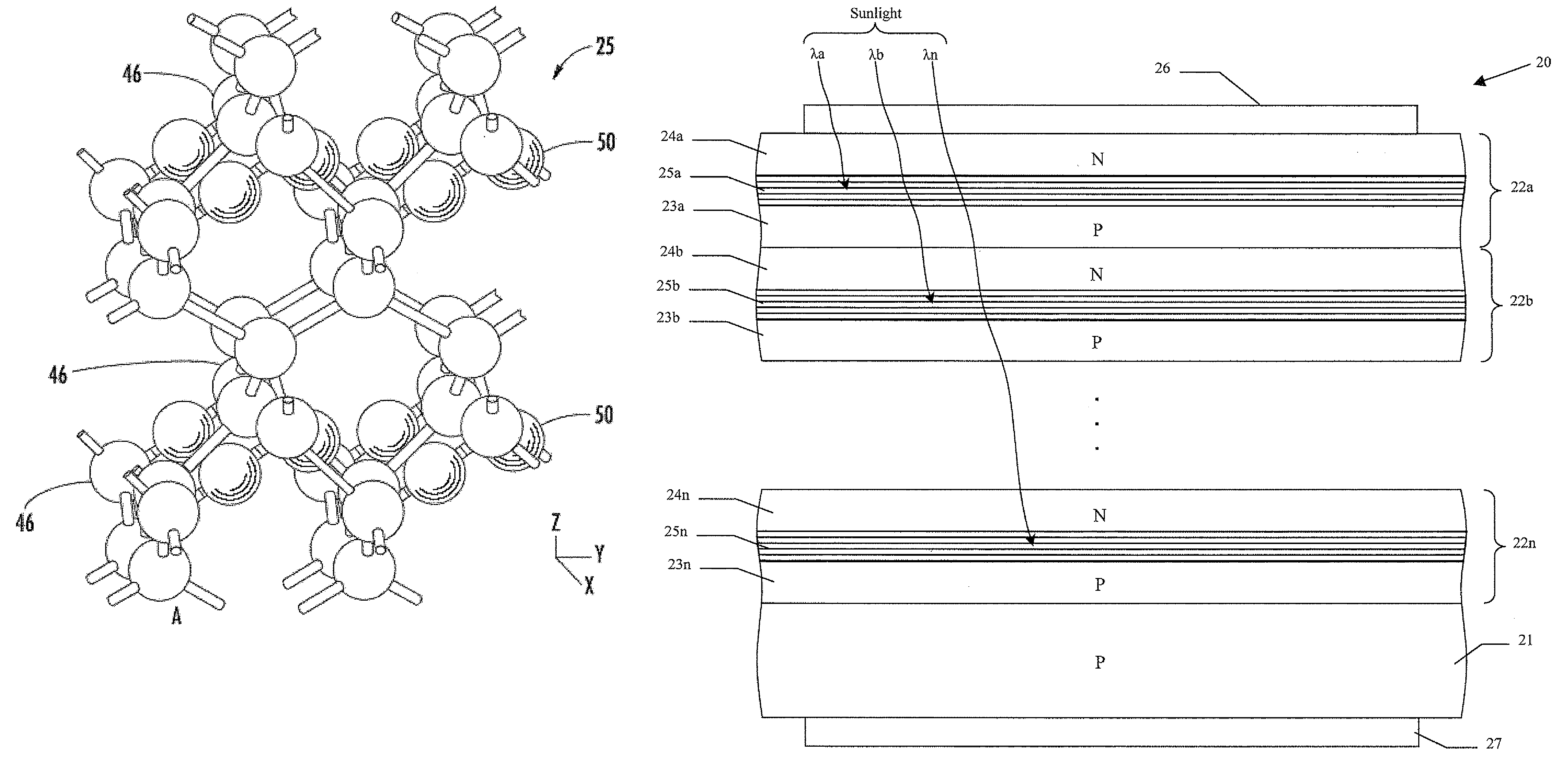
[0012]In view of the foregoing background, it is therefore an object of the present invention to provide a method for making a multiple-wavelength opto-electronic device having enhanced mobility characteristics.

Problems solved by technology

For example, typical optical detectors used in solar (i.e., photovoltaic) cells are made of amorphous silicon and are thus relatively inefficient.
As such, to provide desired power output in many applications a relatively large surface area has to be covered with such solar cells, which may not be practical.

Method used


Image

  • Method for making a multiple-wavelength opto-electronic device including a superlattice
  • Method for making a multiple-wavelength opto-electronic device including a superlattice
  • Method for making a multiple-wavelength opto-electronic device including a superlattice

Examples


Embodiment Construction

[0027]The present invention will now be described more fully hereinafter with reference to the accompanying drawings, in which preferred embodiments of the invention are shown. This invention may, however, be embodied in many different forms and should not be construed as limited to the embodiments set forth herein. Rather, these embodiments are provided so that this disclosure will be thorough and complete, and will fully convey the scope of the invention to those skilled in the art. Like numbers refer to like elements throughout, and prime notation is used to indicate similar elements in different embodiments.

[0028]The present invention relates to controlling the properties of semiconductor materials at the atomic or molecular level. Further, the invention relates to the identification, creation, and use of improved materials for use in semiconductor devices.

[0029]Applicants theorize, without wishing to be bound thereto, that certain superlattices as described herein reduce the ef...


PUM


Abstract

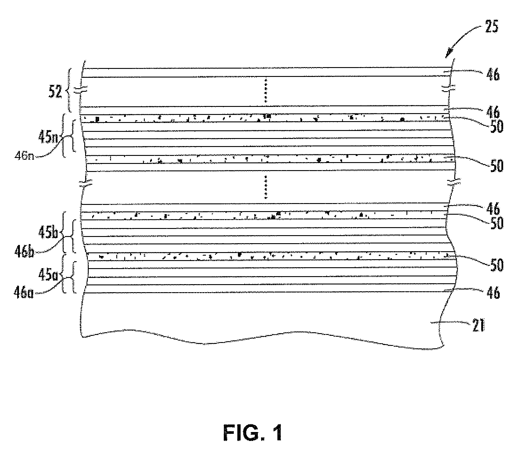
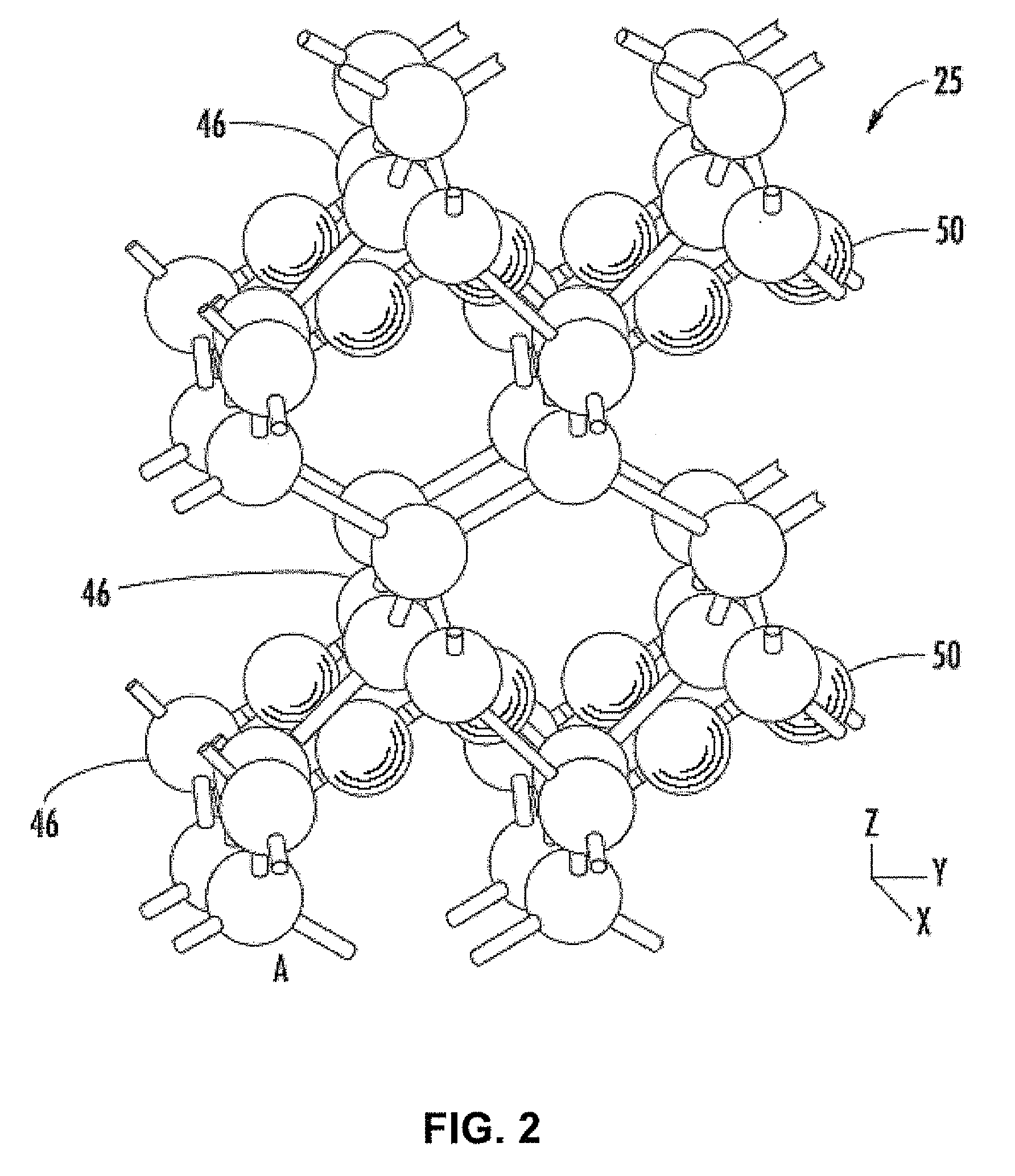
A method for making a multiple-wavelength opto-electronic device which may include providing a substrates and forming a plurality of active optical devices to be carried by the substrate and operating at different respective wavelengths. Moreover, each optical device may include a superlattice comprising a plurality of stacked groups of layers, and each group of layers may include a plurality of stacked semiconductor monolayers defining a base semiconductor portion and at least one non-semiconductor monolayer thereon.

Description

FIELD OF THE INVENTION[0001]The present invention relates to the field of semiconductor devices, and, more particularly, to opto-electronic devices and related methods.BACKGROUND OF THE INVENTION[0002]Structures and techniques have been proposed to enhance the performance of semiconductor devices, such as by enhancing the mobility of the charge carriers. For example, U.S. Patent Application No. 2003 / 0057416 to Currie et al. discloses strained material layers of silicon, silicon-germanium, and relaxed silicon and also including impurity-free zones that would otherwise cause performance degradation. The resulting biaxial strain in the upper silicon layer alters the carrier mobilities enabling higher speed and / or lower power devices. Published U.S. Patent Application No. 2003 / 0034529 to Fitzgerald et al. discloses a CMOS inverter also based upon similar strained silicon technology.[0003]U.S. Pat. No. 6,472,685 B2 to Takagi discloses a semiconductor device including a silicon and carbon...

Claims


Application Information

Patent Timeline
Patent Type & Authority Patents(United States)
IPC IPC(8): H01L21/00H01L33/06
CPCB82Y20/00H01L31/035236H01L31/0725H01L31/18H01L33/06H01L31/022466H01L31/028H01L31/0304H01L31/1884Y02E10/50
Inventor MEARS, ROBERT J.STEPHENSON, ROBERT JOHNHYTHA, MAREKDUKOVSKI, ILIJAYIPTONG, JEAN AUGUSTIN CHAN SOW FOOKHALILOV, SAMEDHUANG, XIANGYANG
Owner ATOMERA INC
Learn More