Formulations for voltage switchable dielectric material having a stepped voltage response and methods for making the same

a voltage switchable technology, applied in the field of overvoltage protection, can solve the problems of affecting or destroying the semiconductor die or chip of the semiconductor device, the voltage switchable dielectric material manufactured in this way can begin to leak current at normal operating voltage, and the difficulty of manufacturing such voltage switchable dielectric materials

Inactive Publication Date: 2011-01-18
LITTELFUSE INC
View PDF220 Cites 37 Cited by
  • Summary
  • Abstract
  • Description
  • Claims
  • Application Information

AI Technical Summary

Problems solved by technology

Semiconductor devices comprising a semiconductor die or chip are easily affected or destroyed by over-voltage events.
Line transients include power surges on AC power lines, and can also be caused by events such as closing a switch or starting a motor.
Unfortunately, voltage switchable dielectric materials manufactured in this way can begin to leak current at normal operating voltages.
Also, manufacturing such voltage switchable dielectric materials can be problematic.
The metal particles must be uniformly dispersed throughout the polymer and small concentration variations can significantly diminish the properties or produce unacceptable variations in electrical properties.
While uniformity can be improved with long mixing times, long mixing times are undesirable for numerous reasons including the cost.

Method used


Image

  • Formulations for voltage switchable dielectric material having a stepped voltage response and methods for making the same
  • Formulations for voltage switchable dielectric material having a stepped voltage response and methods for making the same
  • Formulations for voltage switchable dielectric material having a stepped voltage response and methods for making the same

Examples


Embodiment Construction

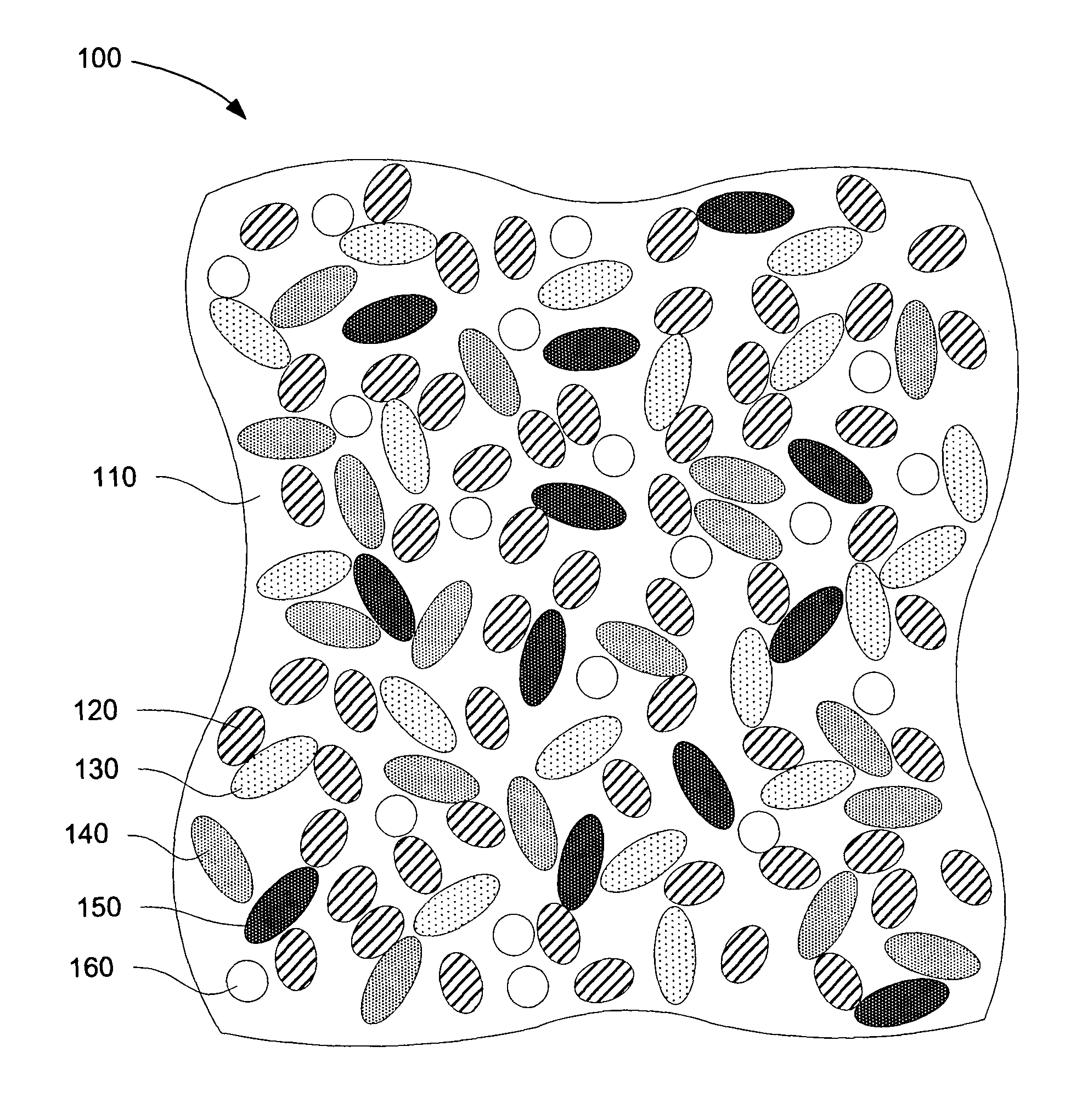
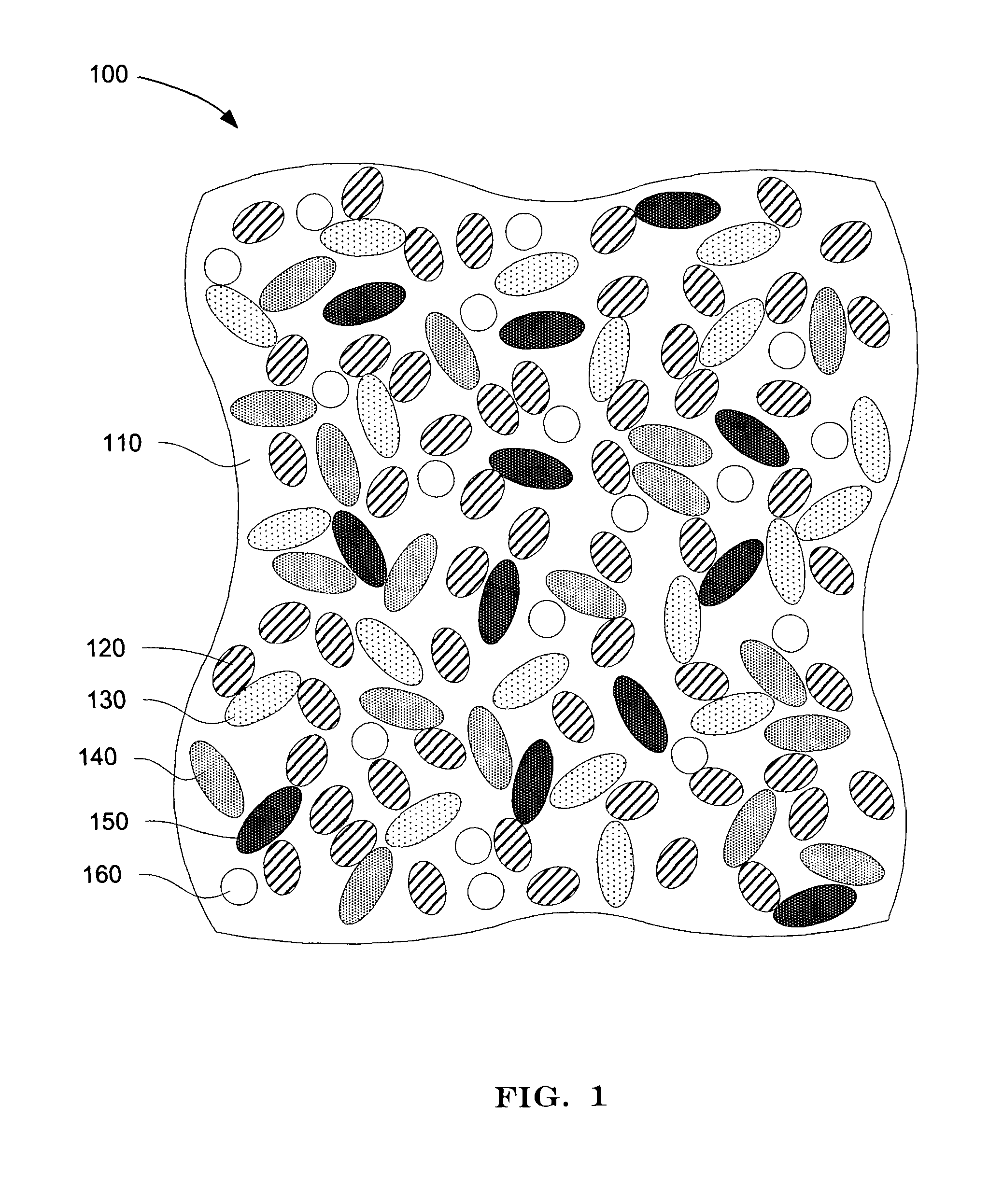
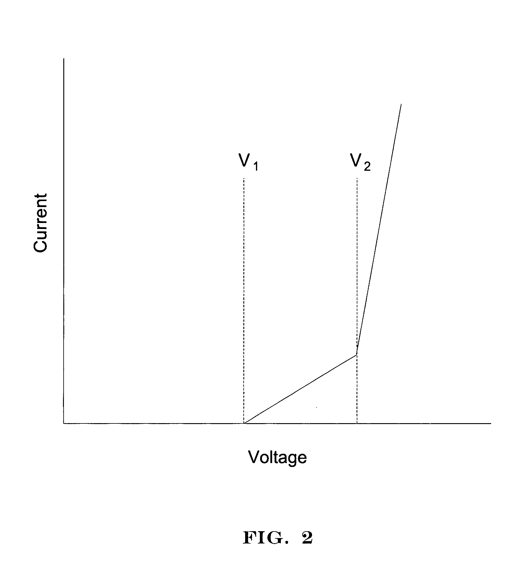
[0017]The present invention provides formulations for voltage switchable dielectric materials. The formulations are characterized by two or more different types of semiconductive materials distributed within a dielectric matrix material. The semiconductive materials are selected to have different bandgap energies in order to provide the resulting voltage switchable dielectric material with a stepped response to different levels of over-voltages. The semiconductive materials can take the form of particles, but are not limited thereto. Alternatively, a semiconductive material can be soluble in, or miscible with, the dielectric matrix material. Formulations optionally can also include electrically conductive and / or insulating materials. In some embodiments, at least one of the conductive or semiconductive materials comprises particles characterized by an aspect ratio of at least 3 or greater. Such high aspect ratio particles allow for an overall reduction of the volume percentage of co...


PUM

PropertyMeasurementUnit
bandgap energyaaaaaaaaaa

Abstract

Formulations for voltage switchable dielectric materials include two or more different types of semiconductive materials uniformly dispersed within a dielectric matrix material. The semiconductive materials are selected to have different bandgap energies in order to provide the voltage switchable dielectric material with a stepped voltage response. The semiconductive materials can comprise inorganic particles, organic particles, or an organic material that is soluble in, or miscible with, the dielectric matrix material. Formulations optionally can also include electrically conductive materials. At least one of the conductive or semiconductive materials in a formulation can comprise particles characterized by an aspect ratio of at least 3 or greater.

Description

CROSS-REFERENCE TO RELATED APPLICATIONS[0001]This application claims the benefit of U.S. Provisional Application No. 60 / 826,747 entitled “Voltage Switchable Device and Dielectric Material with Stepped Bandgap Containing Particles” and filed on Sep. 24, 2006, which is incorporated by reference herein. This application is related to U.S. application Ser. No. 11 / 829,948 entitled “Voltage Switchable Dielectric Material having High Aspect Ratio Particles” and filed on Jul. 29, 2007, and U.S. application Ser. No. 11 / 829,946 entitled “Voltage Switchable Dielectric Material having Conductive or Semi-Conductive Organic Material” and also filed on Jul. 29, 2007, both of which are incorporated by reference herein.BACKGROUND OF THE INVENTION[0002]1. Field of the Invention[0003]The present invention relates generally to the field of electronic devices and more particularly to over-voltage protection.[0004]2. Related Art[0005]Semiconductor devices comprising a semiconductor die or chip are easily...

Claims


Application Information

Patent Timeline
Patent Type & Authority Patents(United States)
IPC IPC(8): H01L47/00
CPCB82Y30/00H01C7/12H01L21/312Y10S438/90H01L21/3148H01L21/318H01L21/02175H01L21/02167H01L21/02118H01L21/02126H01B1/14H01L21/02112
Inventor KOSOWSKY, LEXFLEMING, ROBERT
Owner LITTELFUSE INC
Why Eureka
Try Eureka