Method to make integrated device using oxygen ion implantation

a technology of oxygen ion and integrated device, which is applied in the field of spinelectronic devices, can solve the problems of increasing the cost of increased write current, reducing the write current, and not having enough magnetic crystalline anisotropy to achieve thermally stable perpendicular magnetization, etc., and achieves the effect of effectively capturing oxygen

Inactive Publication Date: 2014-10-16
GUO YIMIN
View PDF2 Cites 5 Cited by
  • Summary
  • Abstract
  • Description
  • Claims
  • Application Information

AI Technical Summary

Benefits of technology

[0018]The present invention is to make magnetic random access memory (MRAM), or integrated device in general. Oxygen ion implantation is used to convert the photolithography exposed areas into metal oxide dielectric matrix. To confine the oxygen ions within the desired region, heavy metals with large atomic number, such as Hf, Ta, W, Re, Os, Ir, Pt, Au is used as ion mask and bottom ion-stopping layer. An oxygen gettering material, selected from Mg, Zr, Y, Th, Ti, Al, Ba is added above and below the active device region to effectively capture the impinging oxygen. After a high temperature anneal, a buried metal oxide layer with sharp oxygen boundaries across the active device region can be obtained.

Problems solved by technology

However, where a MTJ is formed as a device of a perpendicular magnetization type, the materials of the recording layer typically used in an in-plane MTJ for both high MR and low damping constant as required by low write current application normally don't have enough magnetic crystalline anisotropy to achieve thermally stable perpendicular magnetization against its demagnetization field.
Doing so, reduction in write current becomes difficult due to the fact that damping constant increases from the additional perpendicular magnetization layer and its associated seed layer for crystal matching and material diffusion during the heat treatment in the device manufacturing process.
Although a high perpendicular anisotropy is preferred in term of a high thermal disturbance resistance, an increased write current is expected as a cost.
More, even when the tunnel barrier does not immediately break down, if recording operations are repeated, the element may still become nonfunctional such that the resistance value changes (decreases) and information readout errors increase, making the element un-recordable.
Furthermore, recording is not performed unless a sufficient voltage or sufficient spin current is applied.
Accordingly, problems with insufficient recording arise before possible tunnel barrier breaks down.
However, making of small MTJ element leads to increasing variability in MTJ resistance and sustaining relatively high switching current or recording voltage variation in a STT-MRAM.
The MTJ patterning process becomes one of the most challenging aspects of manufacturing.
Conventional techniques utilized to pattern small dimensions in a chip, such as ion milling etching (IBE) or reactive ion etching (RIE), having been less than satisfactory when applied to magnetic tunnel junction stacks used for MRAM.
In most cases when these techniques are used, it is very difficult or almost impossible to cleanly remove etched materials without partial damages to magnetic tunnel junction properties and electric current shunting.
In a RIE etching of magnetic material, physical sputtering is still the major component which unavoidable results in the formation of re-deposited residues that can short circuit the junctions of the MTJ or create shunting channel of the MTJ, yielding high resistance variations and serious reliability issues.
Another problem of conventional patterning techniques is the degradation of the recording layer and reference layer in the MTJ, due to corrosion caused by chemical residue remaining after etching.
Exposure to reactive gases during refilling deposition of dielectrics such as silicon dioxide or silicon nitride after the MTJ etching can also cause corrosion.
After refilling of dielectric material, a chemical mechanic polishing process is required to smooth out the top surface for bit line fabrication, which introduces a big manufacturing challenging as well as high cost and further corrosion.
As the result, the formed sensor size cannot be made small enough to reduce the current for information writing.
Often the etched sensor edge got damaged with electrical shorting across the MgO barrier (220).

Method used


Image

  • Method to make integrated device using oxygen ion implantation
  • Method to make integrated device using oxygen ion implantation
  • Method to make integrated device using oxygen ion implantation

Examples


Embodiment Construction

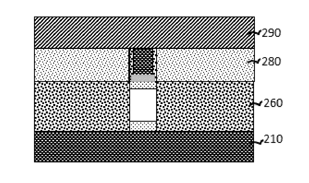
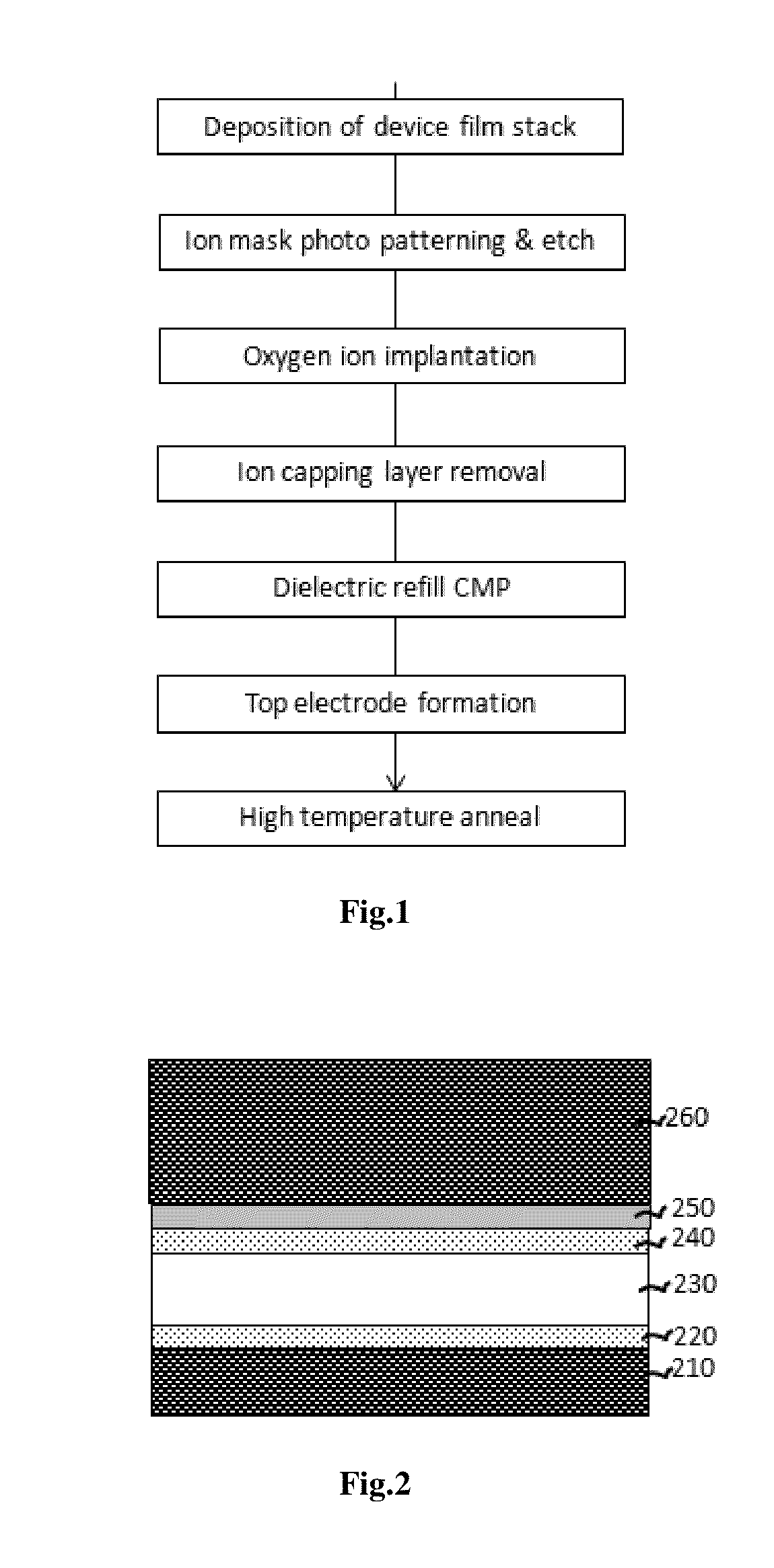
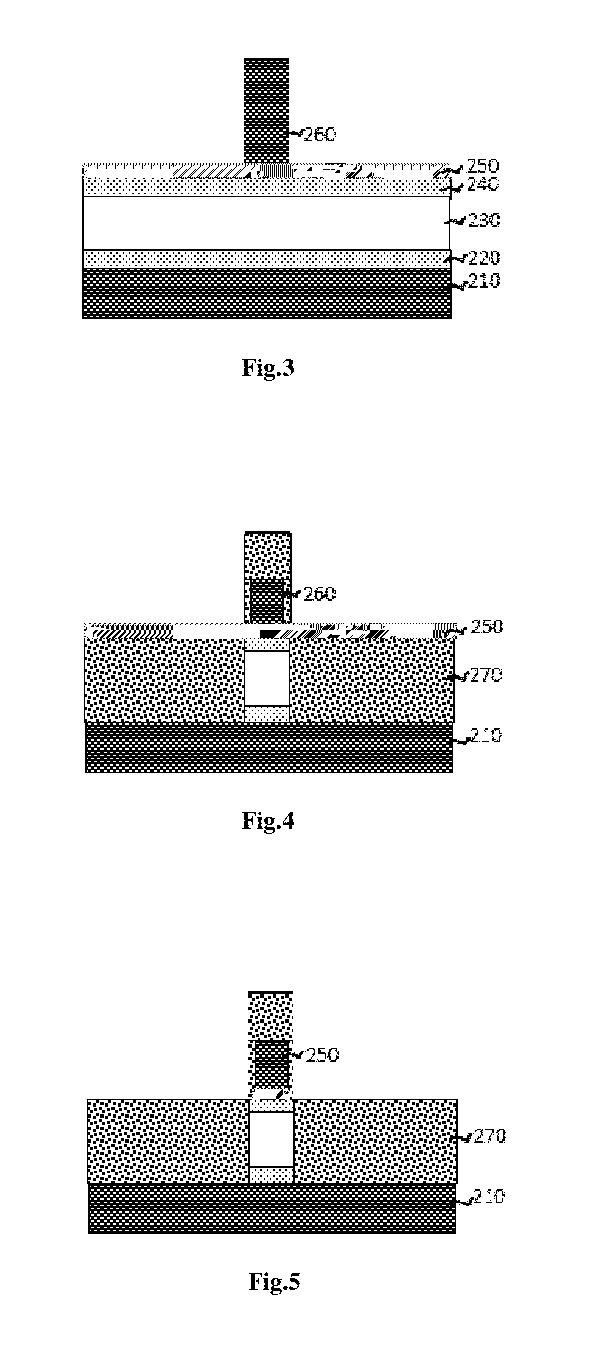
[0032]Here we use oxygen ion implantation to convert the photolithography exposed areas into metal oxide thus forming an electric insulating dielectric matrix. The process flow is shown in FIG. 1. The first operation is to deposit device film stack on a Si substrate which may already contains CMOS control circuits. In general, the process described here can be used to make any type of integrated devices, such as diodes, FETs, and various RAMs including MRAM. The film (FIG. 2) stack contains several key layers, a bottom ion-stopping layer (210), an oxygen gettering layer (220), a device layer (230) which could contains a series of sub-layers, another oxygen gettering layer (240), an ion-capping layer (250), and an ion-mask layer (260).

[0033]The ion-stopping layer (210) typically contains a heavy metal with large atomic number, selected from Hf, Ta, W, Re, Os, Ir, Pt, Au, with a thickness between 200 A-1000 A. Pt or Au is superior to other materials because of their resistance to oxyg...


PUM


Abstract

A method to make magnetic random access memory (MRAM), or integrated device in general, is provided. Oxygen ion implantation is used to convert the photolithography exposed areas into metal oxide dielectric matrix. To confine the oxygen ions within the desired region, heavy metals with large atomic number, such as Hf, Ta, W, Re, Os, Ir, Pt, Au is used as ion mask and bottom ion-stopping layer. An oxygen gettering material, selected from Mg, Zr, Y, Th, Ti, Al, Ba is added above and below the active device region to effectively capture the impinging oxygen. After a high temperature anneal, a buried metal oxide layer with sharp oxygen boundaries across the active device region can be obtained.

Description

RELATED APPLICATIONS[0001]This application claims the priority benefit of U.S. Provisional Application No. 61,812,238 filed on Apr. 15, 2013, which is incorporated herein by reference.BACKGROUND OF THE INVENTION[0002]1. Field of the Invention[0003]This invention relates generally to spin-electronic devices, more particularly to a magnetic tunnel junction and methods for making the same.[0004]2. Description of the Related Art[0005]Magnetoresistive elements having magnetic tunnel junctions (also called MTJs) have been used as magnetic sensing elements for years. In recent years, magnetic random access memories (hereinafter referred to as MRAMs) using the magnetoresistive effect of MTJ have been drawing increasing attention as the next-generation solid-state nonvolatile memories that can cope with high-speed reading and writing, large capacities, and low-power-consumption operations. A ferromagnetic tunnel junction has a three-layer stack structure formed by stacking a recording layer ...

Claims


Application Information

Patent Timeline
Patent Type & Authority Applications(United States)
IPC IPC(8): H01L43/02H01L43/12
CPCH01L43/12H01L43/02H10N50/01H10B61/00
Inventor GUO, YIMIN
Owner GUO YIMIN
Why Eureka
Try Eureka