Printed temperature sensor

a temperature sensor and printed technology, applied in the direction of resistor mounting/supporting, instruments, heat measurement, etc., can solve the problems of limited number of micro-particles forming the conductive path, unsuitable for low temperature processing difficult to negatively affect the thermoelectrical properties of ceramic based ntc, etc., to achieve the effect of providing mechanical stability of the film

Active Publication Date: 2020-01-16
NEDERLANDSE ORG VOOR TOEGEPAST-NATUURWETENSCHAPPELIJK ONDERZOEK (TNO)
View PDF11 Cites 4 Cited by
  • Summary
  • Abstract
  • Description
  • Claims
  • Application Information

AI Technical Summary

Benefits of technology

[0004]Accordingly, the present disclosure provides a temperature sensor which may be printed on a substrate. The temperature sensor comprises an electrical circuit. The electrical circuit comprises a pair of electrodes. The electrodes are separated by an electrode gap. A sensor material is disposed between the electrodes thus filling the electrode gap. The sensor material comprises semi-conducting micro-particles. The micro-particles comprise of a material with a strong NTC behavior. The micro-particles are mixed in a dielectric matrix which is non-conducting. The dielectric matrix may function as a binder e.g. to make it suitable for printing the sensor material and provide mechanical stability of the film after curing. Advantageously the micro-particles may be individual (unmerged) but contacting each other to form an interconnected network through the dielectric matrix. The interconnected network of micro-particles acts as a conductive pathway with negative temperature coefficient between the electrodes.
[0005]By mixing the NTC material as micro-particles in a suitable dielectric matrix, the material becomes printable. The ceramic micro-particles may be processed at high temperature before forming an ink or paste by mixing with the matrix. The dielectric matrix may be mixed with a solvent that is evaporated after application of the material at low temperatures. By mixing the micro-particles such that they contact each other after application to form an interconnected network in the sensor material, it is found that the thermo-electric properties of the NTC material can be retained without the need to merge the particles by melting or sintering. Accordingly, a printable temperature sensor is provided with reliable thermo-electrical properties which can be applied e.g. to conventional substrates under low temperature conditions.
[0012]By providing the dielectric matrix an electrically insulating material, it may be ensured that conduction essentially only takes place via the NTC material of the micro-particles. For example the dielectric matrix may comprise polymeric or cross-linkable material. By using a material of the dielectric matrix having a neutral pH (potential of Hydrogen, Acidity), the matrix is typically charged neutral ensuring the micro-particles are not deteriorated by the matrix acidity. By using material for the dielectric matrix with a low affinity for humidity, e.g. dense and / or hydrophobic material, environmental effects on the conduction behavior may be avoided. For example the dielectric matrix may form a dense structure after crosslinking, e.g. allowing a maximum water uptake of less than half (mass) percent, preferably below a tenth of a percent. For example, the dielectric matrix comprises a precursor with an acrylate, epoxy, isoprene or benzocyclobutene moiety. For example, the dielectric matrix comprises a dielectric polymer such as polyurethane ether, polyisoprene, cellulose nitrate.
[0013]The electrodes are typically made of metal and may be deposited e.g. via sputtering of metals such as Al, Mo, Ag, Au, Cu. Preferably though, the electrodes are also printed, e.g. made from a silver paste or ink, or copper. For example the electrodes may have a layer thickness in a range between 0.1 to 10 μm. By forming an interdigitated finger electrode (driver) the electrode gap can relatively long transverse to the gap distance, e.g. at least ten times a minimum gap distance. This may lower the overall resistance of the sensor, which is preferably in a range between 10 kΩ and 10 MΩ. For example a film of sensor material may be formed between the electrode fingers with a cross-sectional area larger than 0.01 mm2. For example, the cross-sectional area is as a product of the width and height of the film. Optionally, a resistance of the sensor layer can trimmed, e.g. by a laser to match a predetermined value within some percentage, e.g. 10%.
[0014]Optionally the ceramic particles may be shaped during sintering into filaments. In this way, filaments or nanowires can be created with high aspect ratio enabling high conductivity in the direction of the filaments.

Problems solved by technology

Making a ceramic based NTC suitable for low temperature processing is difficult without negatively affecting its thermo-electrical properties.
In general, current high reliability thermistors require high temperature processing which makes it unsuitable for printing on widespread substrates in electronics, e.g. plastics such as PEN / PET, rubbers such as silicones or polyurethanes, composites boards such as FR4, high temperature foils e.g. polyimide or glass.
By using a relatively narrow gap with NTC material between the electrodes, the number of micro-particles forming the conductive path may be limited.

Method used


Image

  • Printed temperature sensor
  • Printed temperature sensor
  • Printed temperature sensor

Examples


second embodiment

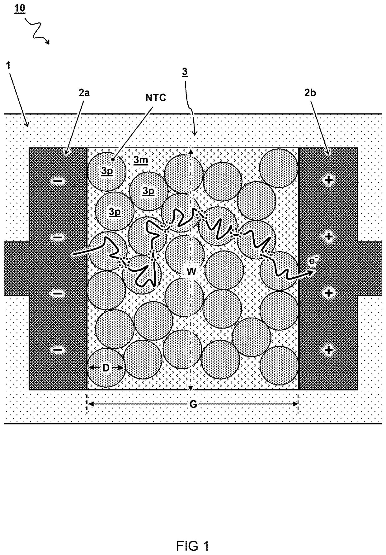
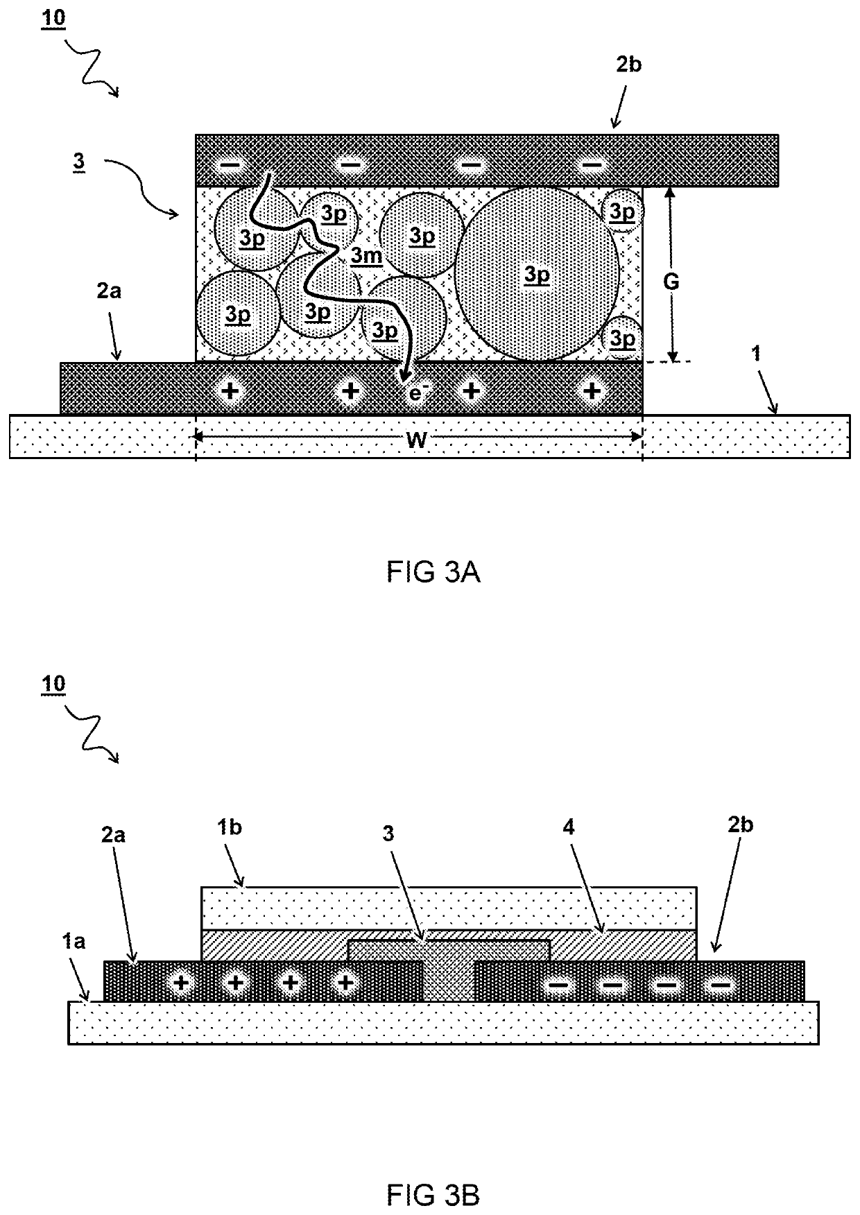
[0051]FIG. 3A schematically illustrates a side view of a second embodiment for a sensor 10. In the embodiment shown, the sensor 10 is formed by a vertical stack on the substrate 1. The stack comprises a layer of sensor material 3 deposited between layers forming a bottom electrode 2a and top electrode 2b. Accordingly, a distance of the electrode gap G may be determined by a layer thickness of the sensor material 3.

third embodiment

[0052]FIG. 3B schematically illustrates a side view of a third embodiment for a sensor 10. In the embodiment shown, the sensor material 3 between the electrodes 2a,2b is encapsulated by an encapsulation layer 4. In one embodiment, the substrate 1 is formed by two parts 1a, 1b on both sides of the sensor material 3.

fourth embodiment

[0053]FIG. 4A schematically illustrates a top view of a fourth embodiment for a sensor 10. In the embodiment shown, the electrodes 2a,2b form an intertwined finger structure defining an elongated meandering gap G with sensor material 3 there between. In one embodiment, the elongated gap has a gap length transverse to the electrode surfaces, wherein the gap length is at least ten times a minimum gap distance.

[0054]FIG. 4B schematically illustrates a side view of an embodiment for a flexible substrate 1, in this case with multiple sensors 10. In one embodiment, the substrate 1 with one or more sensors 10 is flexible, e.g. allowing a bending radius “r” of less than five millimeters without (the sensors) losing essential functionality. In another or further embodiment, the substrate 1 with one or more sensors 10 is stretchable, e.g. allowing an elongation of a least ten percent without losing essential functionality. For example, the substrate comprises a rubber substrate, e.g. with pol...


PUM

PropertyMeasurementUnit
diameteraaaaaaaaaa
temperatureaaaaaaaaaa
diameteraaaaaaaaaa

Abstract

A printed temperature sensor (10) comprising a substrate (1) with an electrical circuit (2) comprising a pair of electrodes (2a, 2b) separated by an electrode gap (G). A sensor material (3) is disposed between the electrodes (2a, 2b) to fill the electrode gap (G), wherein the sensor material (3) comprises semi-conducting micro-particles (3p) comprising an NTC material with a negative temperature coefficient (NTC), wherein the micro-particles (3p) are mixed in a dielectric matrix (3m) functioning as a binder for printing the sensor material (3); wherein the micro-particles (3p) contact each other to form an interconnected network through the dielectric matrix (3m), wherein the interconnected network of micro-particles (3p) acts as a conductive pathway with negative temperature coefficient between the electrodes (2a, 2b).

Description

TECHNICAL FIELD AND BACKGROUND[0001]The present disclosure relates to a printed temperature sensor based on a resistor with negative temperature coefficient (NTC).[0002]A thermistor is a type of resistor whose resistance has a particular dependence on temperature. When the dependence is known, the resistance can be used as a measure for the temperature. Temperature sensing circuits commonly use a thermistor of the NTC type where its resistance decreases as temperature rises since they provide a sufficiently linear dependence of resistance with temperature. NTC materials used for such thermistor typically comprises a ceramic material. However such materials require special ceramic substrates (alumina, quartz) that can withstand the sintering processes at more than thousand degrees Celsius. Making a ceramic based NTC suitable for low temperature processing is difficult without negatively affecting its thermo-electrical properties. In general, current high reliability thermistors requi...

Claims


Application Information

Patent Timeline
Patent Type & Authority Applications(United States)
IPC IPC(8): H01C7/04H01C17/065H01C1/01G01K7/16
CPCH01C7/049H01C17/06533H01C7/043H01C17/06586H01C1/01G01K7/16
Inventor RENTROP, CORNELIS HERMANUS ARNOLDUSSWEELSSEN, JORGENSAALMINK, MILANSMITS, EDSGER CONSTANT PIETERGROEN, WILHELM ALBERT
Owner NEDERLANDSE ORG VOOR TOEGEPAST-NATUURWETENSCHAPPELIJK ONDERZOEK (TNO)
Why Eureka
Try Eureka