Wiring substrate, manufacturing method thereof, and semiconductor device

a manufacturing method and semiconductor technology, applied in the direction of printed circuit assembling, printed circuit manufacture, basic electric elements, etc., can solve the problems of increasing the cost of a semiconductor device, affecting the yield of semiconductor devices, and being difficult to directly mount such a semiconductor chip on the build-up wiring board, etc., to achieve low cost, high yield, and easy manufacturing

Active Publication Date: 2011-03-08
SHINKO ELECTRIC IND CO LTD
View PDF12 Cites 21 Cited by
  • Summary
  • Abstract
  • Description
  • Claims
  • Application Information

AI Technical Summary

Benefits of technology

It is an object of the present invention to provide a wiring_substrate in which the layer number of wiring patterns can be set to necessary minimum in accordance with a specification of the silicon interposer, and the manufacturing steps are simplified to be manufactured at low cost and with high yield, and it has a high reliability, in the wiring substrate in which a silicon interposer is built, and a manufacturing method thereof, and a semiconductor device.
In the present invention, the unit wiring boards having the wiring patterns which enable the electrical connection between the upper and lower sides are used as one unit, and are stacked on and connected to each other to construct the base wiring board. Thus, unlike the build-up wiring board of the prior art, when the layer number of wiring layers is increased, it is not necessary to symmetrically form the wiring patterns on both surfaces of the core substrate taking the prevention of warping into consideration. Additionally, the base wiring board can be constructed with the necessary minimum layer number of wiring patterns in accordance with the specification of the silicon interposer. Therefore, there is no possibility that the increase in cost and the decrease in yield occur due to the formation of unnecessary wiring patterns.
In one preferred mode of the present invention, a mold compound resin containing a large amount of fillers (epoxy resin containing 85 to 90 percent silica filler as an example) is used as the material of the resin portion. The thermal expansion coefficient of the resin portion is 7 ppm / ° C. to 20 ppm / ° C., and the elastic modulus is 15 GPa to 25 GPa. By forming the resin portion from such a resin material, the thermal expansion coefficients between the silicon interposer, the base wiring board and the resin portion can be made to approximate rather that the case of where a general resin material is used. Thus, an occurrence of the warping to the wiring substrate can be suppressed. Furthermore, the resin portion is formed of the resin material having the high elastic modulus. Thereby, the resin portion serves as a substrate which has a high rigidity to integrally support the base wiring board and the silicon interposer.
In this way, according to the present invention, the base wiring board and the silicon interposer are sealed with the resin having the high rigidity to suppress the occurrence of the warping, and thereby the wiring substrate having a high reliability is constructed.
By adopting the method of manufacturing a wiring substrate according to the present invention, the above-described wiring substrate can be easily manufactured. According to the present invention, firstly, a plurality of unit wiring boards are stacked to form the base wiring board. Then, the silicon interposer is connected on the base wiring board to obtain the interposer-attached wiring substrate. Subsequently, the mold die is disposed on the interposer-attached wiring substrate. Thereafter, a resin is filled in the gap between the plurality of unit wiring boards as well as the gap between the base wiring board and the silicon interposer by means of vacuum transfer molding. The use of the vacuum transfer molding enables a resin to be reliably filled in a fine gap even in the case that a mold compound resin containing a large amount of fillers is used.
As described above, the wiring substrate according to the present invention is constructed by disposing the silicon interposer on the base wiring board in which the unit wiring boards are stacked each other, and filling the resin in the gaps thereamong. Accordingly, the wiring substrate is manufactured with low cost and high yield, and a high reliability thereof is obtained.

Problems solved by technology

Since there is a limitation to make the pitch finer between wirings of a build-up wiring board, it has begun to be difficult to directly mount such a semiconductor chip on the build-up wiring board.
As a result, the increase in cost for a semiconductor device and the decrease in the yield thereof tend to occur.
For example, at a time of pulling-out a wiring from a through-hole land of a build-up wiring board so as to dispose an interposer pad to which a silicon interposer is connected, there is a case where the through-hole land becomes an obstacle in the middle of pulling-out the wiring, making it impossible to pull-out the wiring.
At this time, in the case of the build-up wiring board of the prior art, even when the problem can be solved by adding a wiring only on one surface side, it is necessary to symmetrically form the wirings on both surface sides of the core substrate so as to prevent an occurrence of warping, as the result, a problem in which it costs unnecessary expenses is occurs.
As a result, the number of wiring layers becomes enormous in some cases, leading to concerns of the increase in cost and the decrease in yield.

Method used


Image

  • Wiring substrate, manufacturing method thereof, and semiconductor device
  • Wiring substrate, manufacturing method thereof, and semiconductor device
  • Wiring substrate, manufacturing method thereof, and semiconductor device

Examples


Embodiment Construction

Embodiment of the present invention will be explained with reference to the accompanying drawings hereinafter.

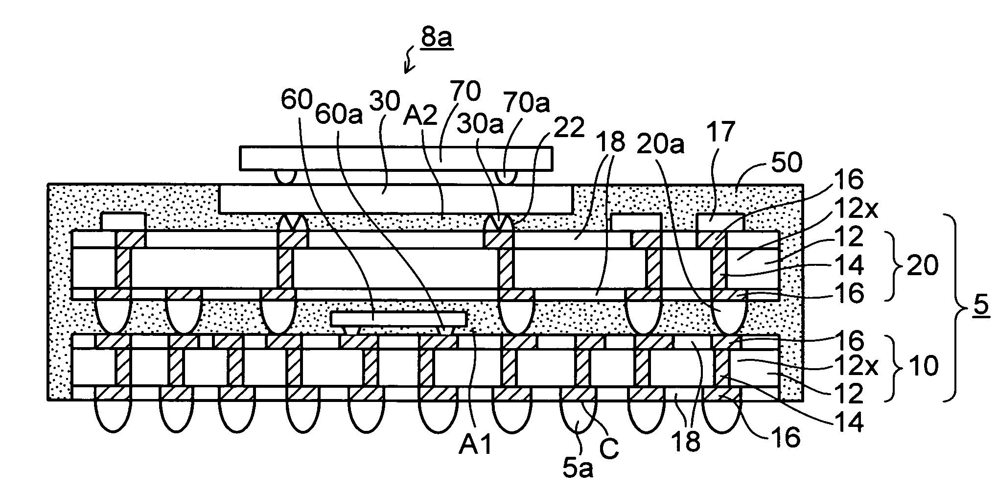
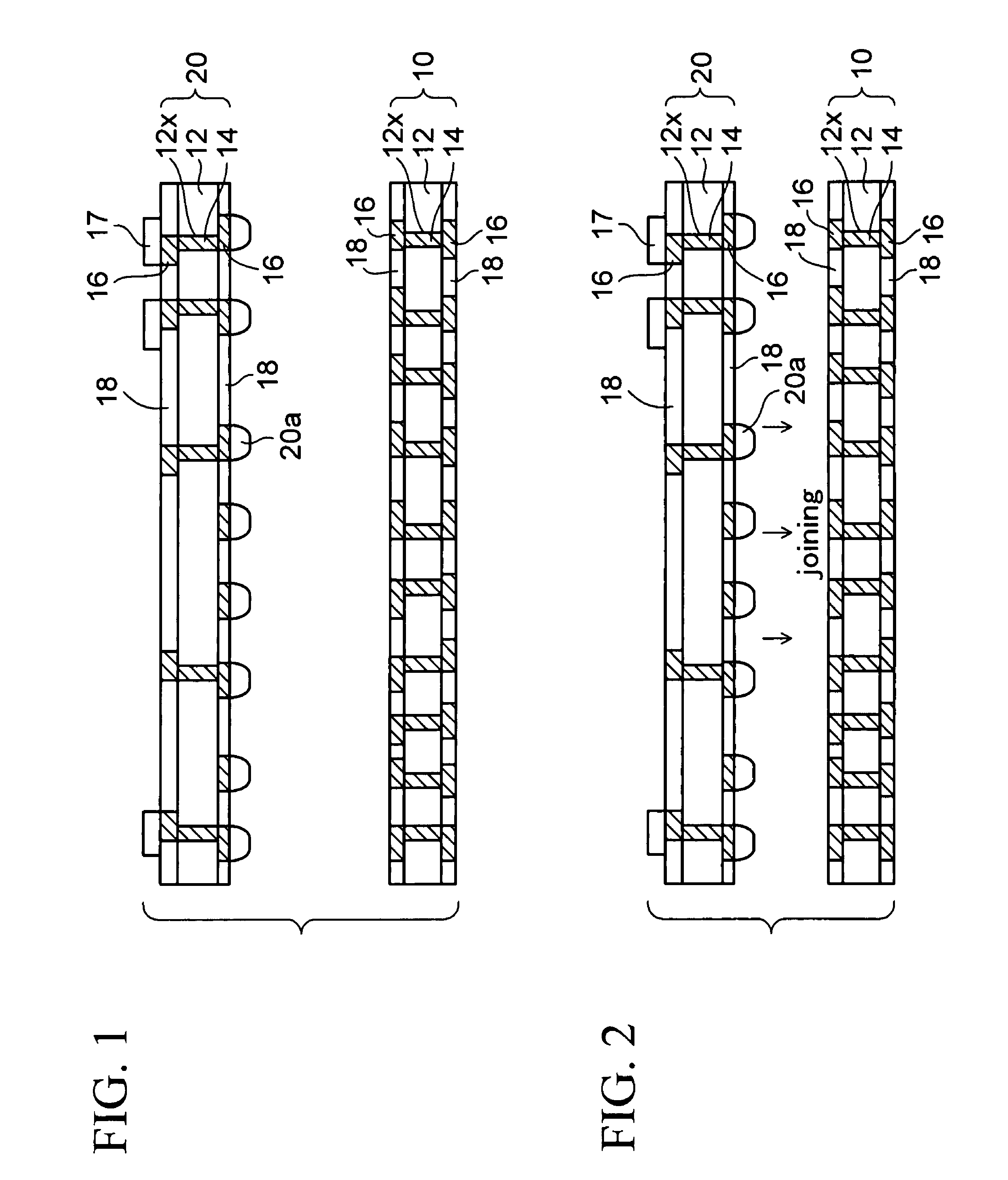
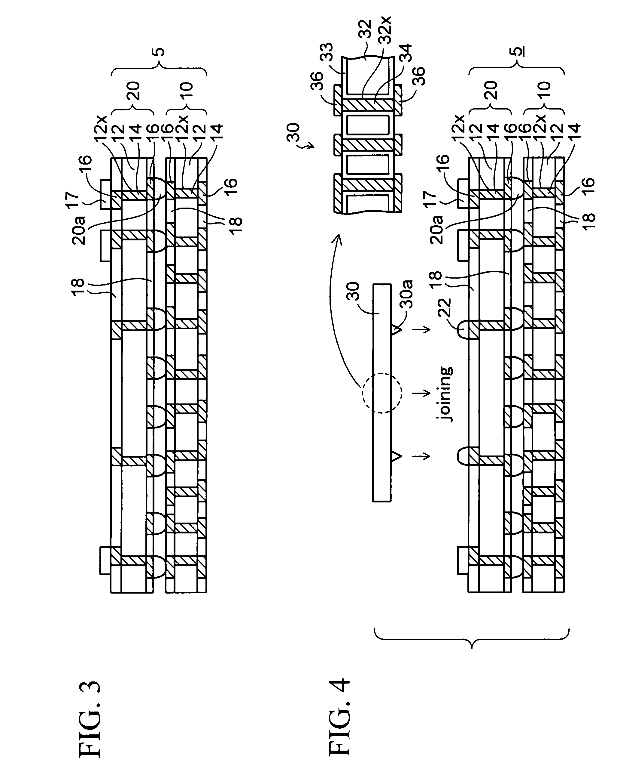
FIGS. 1 to 6 are sectional views each showing a method of manufacturing a wiring substrate according to an embodiment of the present invention, FIGS. 7 to 9 are sectional views each showing a wiring substrate according to an embodiment of the present invention, and similarly, FIGS. 10 and 11 are sectional views each showing a semiconductor device.

Firstly, in the method of manufacturing a wiring substrate according to this embodiment, as shown in FIG. 1, a sheet-like first unit wiring board 10 and a sheet-like second unit wiring board 20 which respectively have wiring patterns 16 which enable electrical connection between the upper and lower sides are prepared. In the first unit wiring board 10, through-holes 12x are formed in an insulating layer 12 which is made of, for example, an epoxy resin (prepreg), or the like, containing glass fabrics. Each through-hole 12x is filled ...


PUM

PropertyMeasurementUnit
elastic modulusaaaaaaaaaa
heightaaaaaaaaaa
widthaaaaaaaaaa

Abstract

In a wiring substrate according to the present invention, a base wiring board is constructed by stacking a plurality of unit wiring boards each having wiring patterns which enable an electrical connection between upper and lower sides, in a state that the plurality of unit wiring boards are connected to each other via a connection terminal, and a silicon interposer is stacked on the base wiring board via a connection terminal, and a resin portion is filled in a gap between the plurality of unit wiring boards as well as a gap between the base wiring board and the silicon interposer, and a resin portion serves as a substrate which integrates the base wiring board and the silicon interposer.

Description

CROSS-REFERENCE TO RELATED APPLICATIONSThis application is based on and claims priority of Japanese Patent Application No. 2006-351000 filed on Dec. 27, 2006, the entire contents of which are incorporated herein by reference.BACKGROUND OF THE INVENTION1. Field of the InventionThe present invention relates to a wiring substrate, a manufacturing method thereof and a semiconductor device, and particularly relates to a silicon interposer built-in wiring substrate which can correspond to the mounting of a high-performance semiconductor chip and a manufacturing method thereof and a semiconductor device.2. Description of the Related ArtIn the prior art, there has been a semiconductor device in which a semiconductor chip such as a CPU is mounted on a wiring substrate therein. As the wiring substrate on which the semiconductor chip is mounted, a build-up wiring board is generally used in which wirings are formed into multiple layers at fine pitches.In recent years, connection electrodes have...

Claims


Application Information

Patent Timeline
Patent Type & Authority Patents(United States)
IPC IPC(8): H01L21/00
CPCH01L21/565H01L23/3128H01L23/49833Y10T29/49126H01L23/49816H01L23/49827H01L23/50H01L2924/19041H01L2224/16225H01L2924/15311H01L2924/157H01L2924/10253H01L23/147H01L2924/00H01L2224/0554H01L2224/05568H01L2224/05573H01L2924/00014H01L2224/05599H01L2224/0555H01L2224/0556
Inventor ARAI, TADASHIKOBAYASHI, TOSHIO
Owner SHINKO ELECTRIC IND CO LTD
Why Eureka
Try Eureka