Schottky barrier semiconductor device and method for manufacturing the same

a technology of schottky barrier and semiconductor, which is applied in the direction of semiconductor devices, electrical appliances, transistors, etc., can solve the problems of increasing the leak current during an operation at a reverse-direction voltage, the power loss of the sbd cannot be minimized, and the performance of the sbd is deteriorated, so as to achieve the effect of minimizing power loss, minimizing power loss, and satisfying properties in a high-temperature environmen

Inactive Publication Date: 2011-03-08
CENTRAL RESEARCH INSTITUTE OF ELECTRIC POWER INDUSTRY
View PDF17 Cites 17 Cited by
  • Summary
  • Abstract
  • Description
  • Claims
  • Application Information

AI Technical Summary

Benefits of technology

[0026]For the silicon carbide Schottky barrier semiconductor device according to the present invention, the n factor is small, and the Schottky barrier height is in a range where power loss is minimized. Moreover, a thermal treatment at a high temperature is applied after Ta that is a Schottky electrode material is deposited. Consequently, properties in a high-temperature environment are satisfactory, and a resistance against heat generation caused by a surge current or the like can be improved.

Problems solved by technology

One of the challenges for a Schottky barrier power semiconductor device such as an SBD is to reduce power loss during operation, and technical developments therefor have been carried out.
However, in the case a Schottky electrode is formed of Ni or Ti, which has been used as a material of a Schottky electrode, the SBH thereof is approximately 1.6 eV for Ni and 0.8 eV for Ti, and the power loss of the SBD cannot be minimized.
As described above, in the case a thermal treatment is carried out to control the SBH after Ni or Ti is deposited, a value of the n factor becomes greatly larger than 1, which deteriorates the performance of an SBD and increases a leak current during an operation at a reverse-direction voltage for instance.
However, as shown in FIG. 3, the SBH is monotonically reduced to less than 1.0 eV with increasing thermal treatment temperature, and is deviated from the range desired for the reduction of power loss.

Method used


Image

  • Schottky barrier semiconductor device and method for manufacturing the same
  • Schottky barrier semiconductor device and method for manufacturing the same
  • Schottky barrier semiconductor device and method for manufacturing the same

Examples


Embodiment Construction

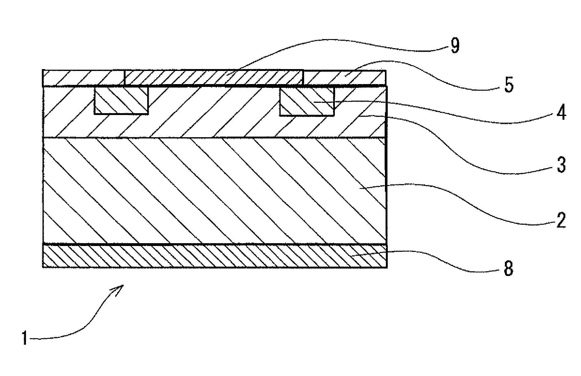
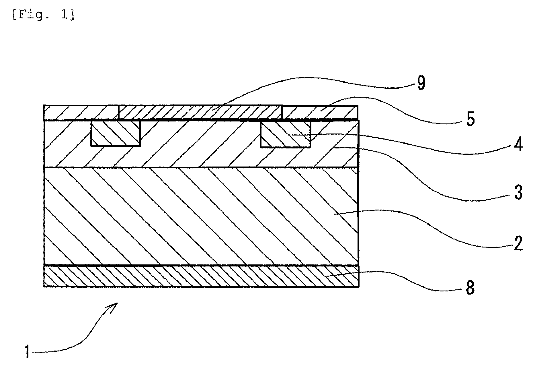
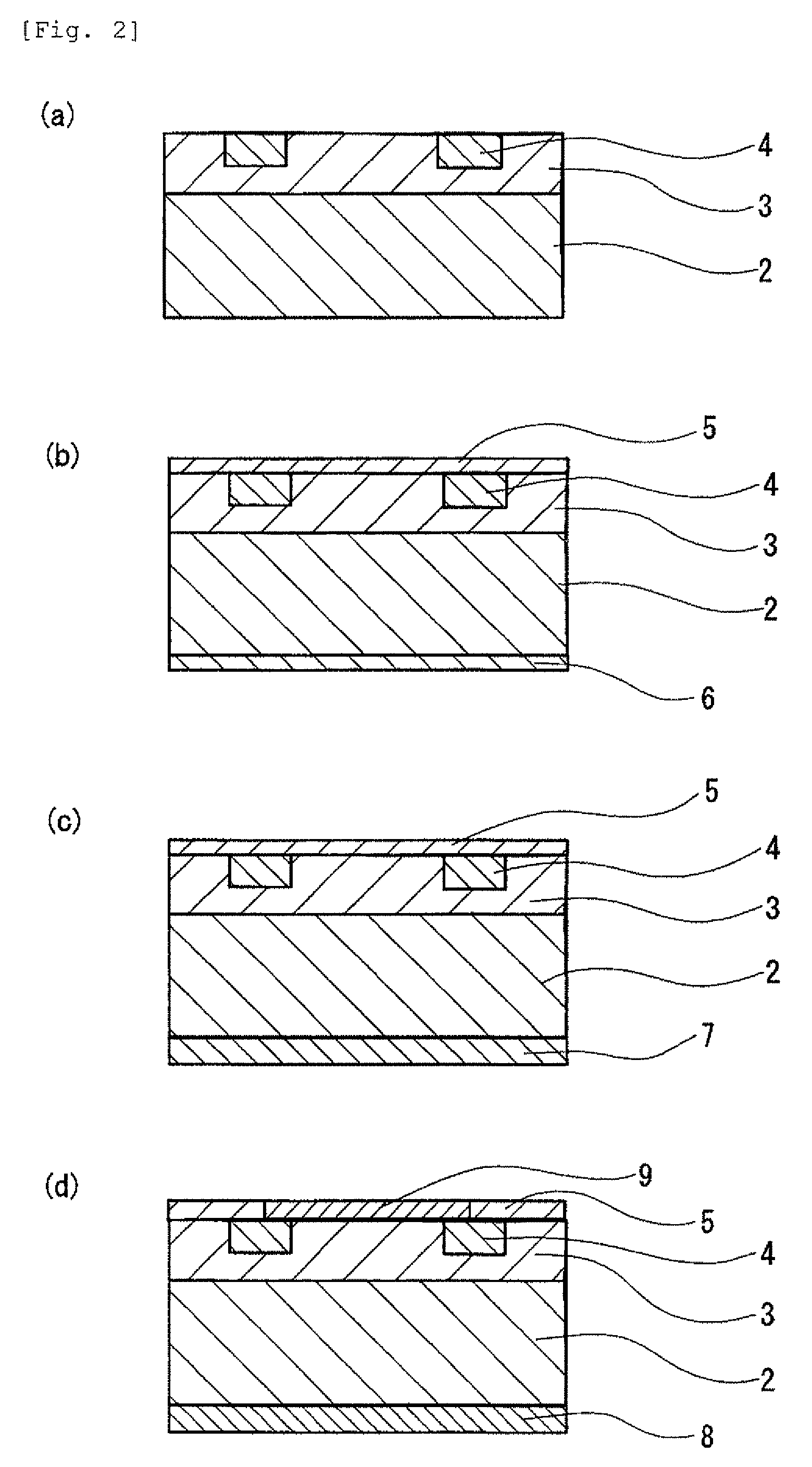
[0030]Embodiments of the present invention will be described below in detail with reference to the drawings. FIG. 1 is a cross-sectional view showing a Schottky barrier diode according to an embodiment of the present invention. A Schottky barrier diode 1 according to the present embodiment is provided with a substrate in which a 4H-SiC epitaxial film 3 is formed on a 4H-SiC single-crystal substrate 2.

[0031]A crystal face on the surface of the SiC epitaxial film 3 is a (000-1) C face, and a Schottky electrode 9 made of Ta is formed on the (000-1) C face.

[0032]On the other hand, a crystal face of the SiC single-crystal substrate 2 opposite to the SiC epitaxial film 3 (hereafter referred to as “rear face”) is a (0001) Si face, and an ohmic electrode 8 made of Ni is formed on the (0001) Si face.

[0033]An ion implantation layer 4 is formed in a peripheral section of the Schottky electrode 9. The ion implantation layer 4 is introduced to relax an electric field concentration to improve wit...


PUM

PropertyMeasurementUnit
inclined angleaaaaaaaaaa
temperatureaaaaaaaaaa
withstand voltageaaaaaaaaaa

Abstract

A silicon carbide Schottky barrier semiconductor device provided with a Ta electrode as a Schottky electrode, in which the Schottky barrier height is controlled to a desired value in a range where power loss is minimized without increasing the n factor. The method for manufacturing the silicon carbide Schottky barrier semiconductor device includes the steps of depositing Ta on a crystal face of an n-type silicon carbide epitaxial film, the crystal face having an inclined angle in the range of 0° to 10° from a (000-1) C face, and carrying out a thermal treatment at a temperature range of 300 to 1200° C. to form the Schottky electrode.

Description

TECHNICAL FIELD[0001]The present invention relates to a Schottky barrier semiconductor device provided with a Schottky electrode on a surface of a silicon carbide epitaxial film and a method for manufacturing the Schottky barrier semiconductor device.BACKGROUND ART[0002]Silicon carbide (SiC) is a semiconductor having excellent physical properties such as an approximately three times larger band gap, an approximately two times larger saturated drift velocity, and an approximately ten times larger dielectric breakdown field strength compared with silicon (Si). Consequently, silicon carbide has been developed as a material of a power semiconductor device, and a Schottky barrier diode (SBD) manufactured with SiC is now commercially available.[0003]The SBD is composed of a SiC single-crystal substrate which is a slice in a wafer shape from a SiC bulk single-crystal grown by a sublimation method or the like, a SiC epitaxial film grown from a surface of the SiC single-crystal substrate by ...

Claims


Application Information

Patent Timeline
Patent Type & Authority Patents(United States)
IPC IPC(8): H01L21/425H01L27/082
CPCH01L21/0495H01L29/045H01L29/66143H01L29/872H01L29/1608H01L29/47
Inventor TSUCHIDA, HIDEKAZUNAKAMURA, TOMONORIMIYANAGI, TOSHIYUKI
Owner CENTRAL RESEARCH INSTITUTE OF ELECTRIC POWER INDUSTRY
Why Eureka
Try Eureka