Semiconductor device and manufacturing method thereof

a semiconductor and manufacturing method technology, applied in the direction of printed circuit aspects, sustainable manufacturing/processing, final product manufacturing, etc., can solve the problems of insufficient connection reliability, inability to obtain sufficient resin material, and the occasional connection of adjacent bumps via voids to form short circuits, etc., to prevent short-circuiting between bumps, high connection reliability, and stable connection

Active Publication Date: 2011-03-08
GK BRIDGE 1
View PDF39 Cites 86 Cited by
  • Summary
  • Abstract
  • Description
  • Claims
  • Application Information

AI Technical Summary

Benefits of technology

[0026]In accordance with the present invention, 50% or more of the connection portion can be covered by the solder resist, and the occurrence of short-circuiting between bumps can be prevented by making the thickness of the solder resist to be equal to or greater than the thickness of the underfill resin disposed on the solder resist. The electrodes can thereby be stably connected to the electrode pads by way of the bumps, and a semiconductor device having high connection reliability can be obtained.

Problems solved by technology

For this reason, sufficient connection reliability cannot be obtained without further improving the physical properties of the underfill resin.
However, since the viscosity of the resin material increases prior to curing when a filler is included, a problem occurs in which the resin material cannot be sufficiently filled in the gap between the semiconductor element and wiring board.
Also, even if the resin material can be sufficiently filled into the gap, the bumps, electrodes, and electrode pads are plastically deformed by heat stress generated when the device operates or at other times in cases in which, for example, voids are produced in the gap between the semiconductor element and wiring board, or at other times, and there is a risk that adjacent bumps will occasionally become connected via the voids to form a short circuit.
Thus, there are difficult problems in that the modulus of elasticity, the coefficient of thermal expansion, and other physical properties of the underfill resin, and the gap filling characteristics of the resin materials must all be kept at the desired level in order to improve the connection reliability of a semiconductor device.
The above-described problems are predicted to become more significant because the filling distance that the resin material must penetrate is increased and the gap between the semiconductor element and wiring board becomes narrower as the size of LSI increases and the pitch is reduced.

Method used


Image

  • Semiconductor device and manufacturing method thereof
  • Semiconductor device and manufacturing method thereof
  • Semiconductor device and manufacturing method thereof

Examples


examples

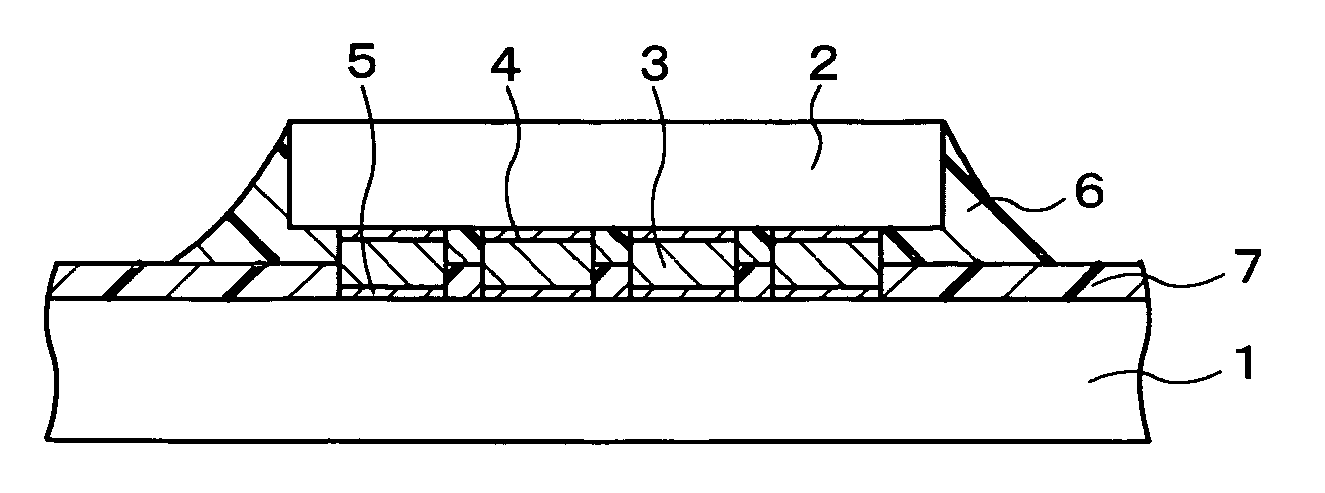
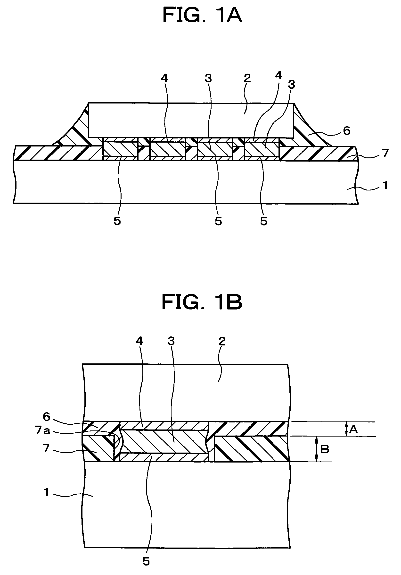
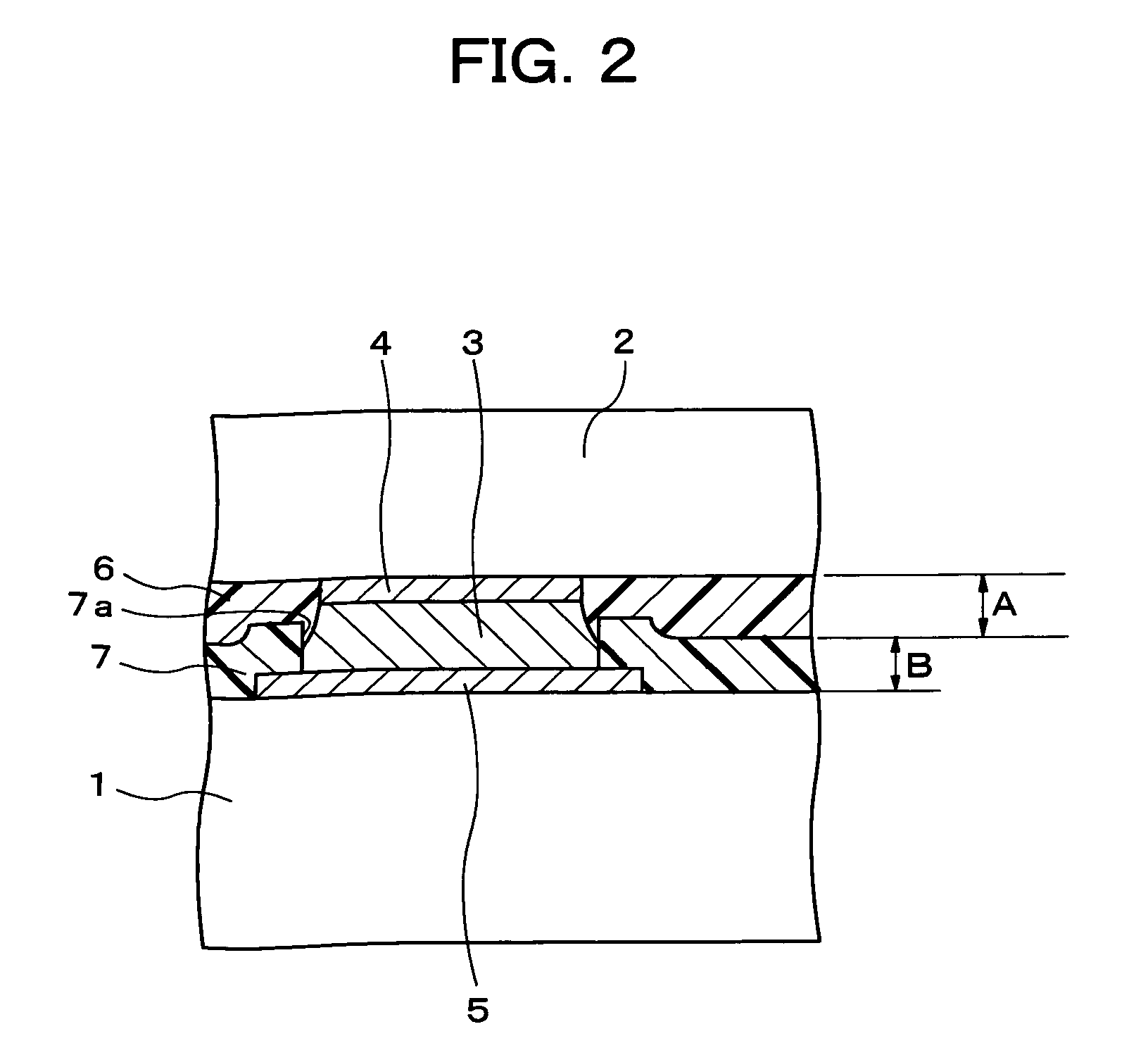
[0079]The effects of the examples of the present invention are described in detail next with reference to comparative examples that are outside the scope of the claims of the present invention. A semiconductor device according to the first embodiment described above was manufactured using the method described in the third embodiment described above. First, a plurality of electrode pads 5 were formed on the surface, as shown in FIG. 3A, and five wiring boards 1 were prepared in which a solder resist 7 was disposed on the periphery of the electrode pads 5. The shape of the wiring boards 1 was square as viewed from above, with a length of 45 mm and a width of 45 mm. The shape of the electrode pads 5 was circular as viewed from above, with a diameter of 135 μm. The array pitch of the electrode pads 5 was 240 μm. A commercially available product manufactured by Tamura Kaken was used as the solder resist 7 of the wiring board 1, and the thickness of the solder resist, i.e., the thickness ...


PUM


Abstract

Electrode pads (5) and a solder resist (7) are disposed on the upper surface of a wiring board (1), and apertures (7a) are formed in the solder resist (7) so as to expose the electrode pads (5). Electrodes (4) are disposed on the lower surface of a semiconductor element (2). Electrodes (4) are connected to the electrode pads (5) by way of bumps (3). An underfill resin (6) is disposed in the area that excludes the solder resist (7) and the bumps (3) in the space between the wiring board (1) and the semiconductor element (2). Between the wiring board (1) and the semiconductor element (2), the thickness (B) of the solder resist (7) is equal to or greater than the thickness (A) of the underfill resin (6) on the solder resist (7). The volume (Vb) of the bumps (3) is less than the volume (Vs) of the apertures (7a).

Description

[0001]This application claims priority from PCT Application No. PCT / JP2005 / 000226 filed Jan. 12, 2005, and from Japanese Patent Application No. 2004-094309 filed Mar. 29, 2004, which applications are incorporated herein by reference.TECHNICAL FIELD[0002]The present invention relates to a semiconductor device in which a semiconductor element is mounted on the wiring board and fabricated by sealing the gap between the semiconductor element and the wiring board with the aid of an underfill resin, and to a manufacturing method thereof; and more particularly relates to a semiconductor device having a flip chip or chip size package, or another mounted structure, and to a manufacturing method thereof.BACKGROUND ART[0003]As electronic equipment becomes more compact, lightweight, and high-performance, flip chip mounting is becoming more widespread as a method for mounting LSI (Large Scale Integrated circuit) chips and other semiconductor elements to a wiring board. Flip chip mounting is a mo...

Claims


Application Information

Patent Timeline
Patent Type & Authority Patents(United States)
IPC IPC(8): H01L23/498H01L21/56H01L21/60H05K3/30H05K3/34
CPCH01L21/563H01L24/16H01L24/32H01L24/81H05K3/305H01L24/29H05K2201/0191H05K2201/0989H05K2201/10674H05K2201/10977H01L24/13H01L2224/13021H01L2224/13099H01L2224/16225H01L2224/27013H01L2224/73203H01L2224/75251H01L2224/81191H01L2224/81192H01L2224/812H01L2224/81801H01L2224/83051H01L2224/83101H01L2224/83192H01L2224/83385H01L2924/01004H01L2924/01005H01L2924/01012H01L2924/01027H01L2924/01029H01L2924/0103H01L2924/01033H01L2924/01047H01L2924/0105H01L2924/01051H01L2924/01078H01L2924/01079H01L2924/01082H01L2924/01322H01L2924/14H05K3/3436H05K3/3452H01L2924/0132H01L2924/01006H01L2924/01019H01L2924/014H01L2924/0133H01L2224/32225H01L2224/73204H01L2224/29111H01L2224/2919H01L2924/00013H01L2224/81193H01L2224/29036H01L2924/01083H01L2224/13111H01L2924/00014H01L2924/00H01L2924/0665H01L2224/29099H01L2224/0554H01L2224/05568H01L2224/05573H01L2224/10175H01L2224/16111H01L2224/16237H01L2224/73104H01L2924/00011H01L2924/351Y02P70/50H01L2224/81805H01L2224/05599H01L2224/0555H01L2224/0556
Inventor OHUCHI, AKIRAMURAKAMI, TOMOO
Owner GK BRIDGE 1
Why Eureka
Try Eureka